


1. INTRODUCTION
Various indium oxide (In2O3) films doped with metals such as molybdenum (Mo) [1, 2] titanium (Ti) [3], zirconium (Zr) [4], tungsten (W) [5], and niobium (Nb) [6] exhibit high visible transmittance (≥ 80%) and low resistivity (≤1×10⁻³cm), and have been applied in various optoelectrical devices including transparent thin film transistors (TTFT) and liquid crystal displays (LCD) [7, 8].
Among all the metal doped In2O3 films, Ti-doped In2O3 (TIO) and Mo-doped In2O3 (MIO) films have received attention because they exhibit high conductivity with rapid carrier mobility [9]. In a previous study, Y. Meng [10] reported a resistivity of 1.6 × 10⁻⁴ Ω cm for 4 at. % Mo-doped In2O3 films and asserted that the high conductivity was due to the substitution of In3+ by Mo6+. In addition, T. Koida reported the enhanced near-infrared transparence of Zr doped In2O3 (ZIO) films, which had a resistivity of 2.6 × 10⁻⁴ Ω cm. The firms were deposited by the RF magnetron co-sputtering of In2O3 and In1.9Zr0.1O3 targets, for thin film solar cells [4]. Also, R. K. Gupta prepared TIO films on sapphire substrate using KrF excimer laser deposition to examine the influence of substrate temperature on the opto-electrical properties of the films. They suggested the optimal temperature of 600 °C, which assured higher carrier mobility than the other temperature conditions [11]. However, such high temperature is not recommended because it may restrict the type of flexible polymer substrate that can be used for bendable optoelectrical devices.
In this study, TIO films were deposited by the radio frequency (RF) magnetron sputtering of a Ti doped In2O3 target, and were then electron beam-irradiated to enhance the opto-electrical properties of the films. Electron beam irradiation with an optimal incident energy assures both low temperature grain growth and flat surface morphology, which will increase visible transmittance [12-14].
2. EXPERIMENTAL PROCEDURES
In this study, an RF (13.56 MHz) magnetron sputter with an electron irradiation system [12] was used to deposit the TIO thin films (thickness; 100 nm) on a slide glass substrate (size; 30 × 30 mm2, Corning 2948) at room temperature. The chamber was evaluated to 5.5 × 10⁻⁷ Torr and then inert argon (Ar) was injected (10 sccm) to maintain a deposition pressure of 1.0 × 10⁻³ Torr. The TIO target was biased with RF 2.5W/cm2 for all depositions.
After deposition, we biased the RF power of 200W on an inductively coupled plasma (ICP) antenna in an electron beam source and varied the electron irradiation energy from 300 to 1500 eV in a low vacuum of 1 × 10⁻⁵ Torr (Ar atmosphere). The variation in grain sizes related to optical transmittance and electrical resistivity was evaluated using an X-ray diffractometer (XRD, XPert-APD, Philips) at the Korea Basic Science Institute (KBSI), Daegu Center. The visible transmittance, sheet resistance, electrical properties, and chemical composition were observed by UV-visible spectrophotometry (Avaspec-2048L, Avantes), four point probe (Loresta-EP, Mitsubishi Chemical), Hall measurement system (HMS-3000, Ecopia) and energy dispersive spectrometer (EDS, JSM-6500F, JEOL), respectively. The bare glass had an optical transmittance of 92% in the visible wavelength region. In addition, the influence of electron irradiation on the surface roughness was investigated using an atomic force microscope (AFM, scan area; 3 × 3 μm2, XE-100, Park Systems).
3. RESULTS AND DISCUSSION
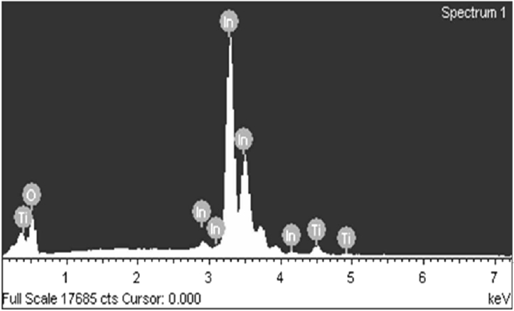
In a previous study, Hest et al. deposited TIO films onto a glass substrate with a combinatorial sputtering system and investigated the relation between Ti doping rate (0-7 at. %) and carrier mobility [15]. It was demonstrated that films doped with 2.8 at. % of Ti showed excellent opto-electrical properties. Thus, we deposited TIO films by RF magnetron sputtering with 3.0 at. % Ti doped In2O3 target. Fig 1 and Table 1 show the observed chemical composition of the films.
Fig 2 shows the XRD patterns observed from the TIO films as a function of electron irradiation energy from 300 to 1500 eV. All of the XRD plots exhibited some diffraction peaks of the cubic bixbyite In2O3 (222), (400), (440), and (622) planes regardless of the electron irradiation energy, while the characteristic diffraction peak for crystalline TiO2 did not appear, even at electron irradiation of 1500 eV. Table 2 shows the observed grain size of the In2O3 (222) plane using the Scherrer equation [16]. The average grain size with electron irradiation at 300, 600, 900, 1200, and 1500 eV were evaluated to be in the order of 9.1, 10.6, 12.5, 14.3 and 15.6 nm. It was concluded that the post-deposition electron irradiation was effective for enhancing the thin film crystallization.
Fig 3 shows a surface image of the TIO films electron irradiated at different energies, with root mean square (RMS) roughness. The RMS roughness of the as deposited films was found to be 0.63 nm. As electron irradiation energy increased up to 1500 eV, the RMS roughness decreased down to 0.36 nm.
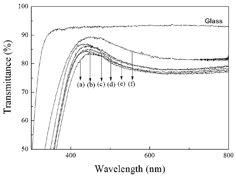
Fig 4 shows the visible transmittance of the as deposited films, and after electron beam irradiation at different energies. The bare glass substrate had an optical transmittance of 93% in the visible wavelength region, while the as deposited film has a lower average visible transmittance of 77.1%. The visible transmittance was enhanced when the electron irradiation energy increased. The average visible transmittance of the films electron-irradiated at 1500 eV was 83.2%. From XRD and AFM observations, it was found that the increased visible transmittance of the TIO films could be attributed to a flatter surface and larger grain size, induced by the postdeposition electron irradiation.
Table 3 shows the dependence of electrical resistivity, carrier density, and mobility on electron irradiation energy. The TIO films electron irradiated at 1500 eV show a higher carrier density of 3.22 × 1020 cm-3. Both carrier density and carrier mobility were enhanced by increases in the electron incident energy. The highest mobility of 30.1 cm2/Vs was observed for TIO films electron irradiated at 1500 eV. The decrease in resistivity (6.4 × 10⁻⁴ Ωcm) with increasing electron irradiation energy was attributed to the enlargement in grain size, as shown in Table 1.
Table 4 shows the compared electrical properties of some impurity doped In2O3 thin films. The Ti doped films showed relatively low resistivity from 5.2 × 10⁻⁴ Ωcm to 7.3 × 10⁻⁴ Ωcm, depending on the deposition method and substrate temperature conditions. In Table 3, even though some Ti and Zr doped films showed lower resistivity than the TIO films prepared in this study, those films were deposited at a relatively high substrate temperature, of 500 °C for the Ti doped films [17] and 650 °C for the Zr doped films [4].
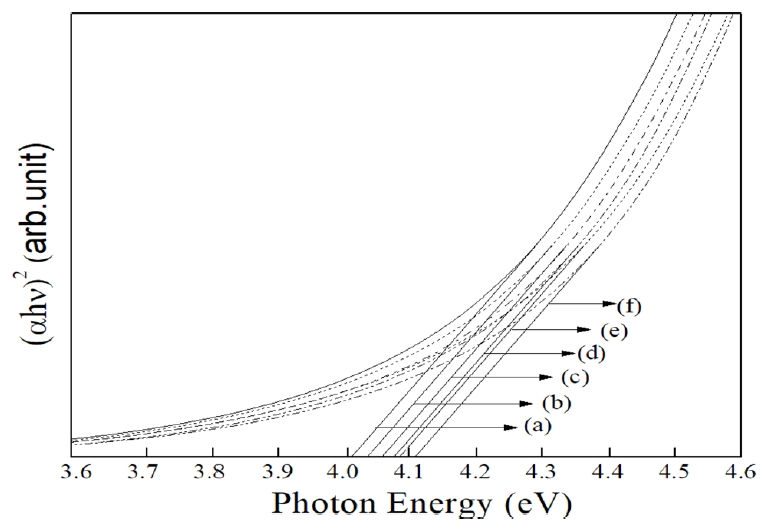
Fig 5 shows a plot of (αhν)2 of the TIO films as a function of the photon energy. The absorption coefficient (α) is evaluated from Eq. (1) [18]:
where t is the thickness and T is the visible transmittance. The Tauc formula in Eq. (2) shows the relationship between the optical absorption coefficient (α) and the optical band gap (Eg) [19]:
where hν is the photon energy and A is the absorption edge width parameter. In Fig 5, the optical band gap increased from 4.013 (at deposition) to 4.108 eV as the electron energy was increased to 1500 eV.
Table 5 shows the carrier density and optical band gap of the TIO films as a function of the electron irradiation energy. From the observed electrical properties and optical band gap, it is concluded that the optical band gap shift is related to the carrier density of the films [20,21]. The band gap was enhanced from 4.013 to 4.108 eV, while the carrier density increased from 9.8 × 10¹⁹ (at deposition) to 3.22 × 1020 cm-3 (at 1500 eV).
4. CONCLUSIONS
Conductive and transparent TIO films were prepared on glass slide substrates using RF magnetron sputtering and then electron beam irradiation, to study the influence of incident electron energy on the visible transmittance, optical band gap, and electrical resistivity of the films. XRD patterns and AFM images showed that the crystallite size increased with electron irradiation energy, and the electron irradiated films at 1500 eV showed the lowest RMS roughness of 0.36 nm. The decrease in resistivity (6.4 × 10⁻⁴ Ωcm) with increasing electron irradiation energy was attributed to the enhanced crystallinity and surface flatness of the films. The results demonstrated that electron beam irradiation effectively improved the optical and electrical performances of the TIO thin films.