


1. Introduction
Most silicon (Si) solar wafers are produced by diamond wire sawing of crystalline silicon (c-Si) ingots. Kerf loss is unavoidable with this diamond wire sawing method. Kerf loss is known to be approximately 50% for a 200 μm thick wafer and increases to approximately 70% as the wafer thickness decreases to 100 μm [1]. Additionally, it is difficult to produce a Si wafer with a thickness of less than 50 um using diamond sawing. However, Mierlo et al. (2017) reported that the Direct Wafer can reduce Si material losses by 50% by preventing kerf loss during wire sawing [2]. Finally, high cost-competition can be achieved by decreasing the wafer cost, which is approximately 60% of the total manufacture cost of c-Si solar cells [3-5]. Kerfless wafering technology has been investigated since 2000 in an effort to overcome the shortcomings of wire sawing. Kerfless wafering is a beneficial technique that enhances the cost effectiveness of crystalline silicon (c-Si) solar cells by preventing silicon (Si) waste during diamond sawing. Kerfless wafering technology has several forms, including lift-off, exfoliation, controlled spalling, and kerf-free wafering. Reported methods include the Stress-induced Lift-off Method (SLIM-cut) [6], the “Epifree” process [7], the seed layer approach [8-10], and ion beam-induced cleaving technology [11,12].
SLIM-cut was developed at IMEC in 2008 and applied to the solar cell [6], and is one of the most widespread kerfless wafering methods. Various materials are used as the stress induced layer (SIL), including silver and aluminum metal paste [13], epoxy [14], and electroplated Ni layer [15]. Stress is induced by the difference in the coefficient of thermal expansion (CTE) between the SIL and the Si mother wafer, and the stress is increased by thermomechanical treatment. A crack is initiated by this stress that propagates parallel to the surface through the sample. As the crack spreads, a thin Si foil is lifted-off from the Si mother wafer. A notch is used to propagate the crack parallel to the surface through the sample during the SLIM-cut method. The notch is a type of crack that is made in the top or the side of an Si wafer [16,17].
In this study, the SLIM-cut method was used to exfoliate a Si foil from a Si mother wafer. Al paste, epoxy, and electroplated Ni layers were used as the SIL and compared. In addition, the notch was applied by laser scribing on the top surface and the side of the wafer. We summarize the Si lift-off processes for Al paste, epoxy, and electroplated Ni layers in Table 1.
2. Experimental Procedures
In this study, we investigated the Si lift-off from a mother wafer using Al paste, epoxy, and electroplated Ni layers as the SIL. A 750 μm-thick Si semiconductor wafer was used as the mother wafer and was cleaned in piranha solution before introducing the SIL. The CTE of the stress-induced material (SIM) should be larger than that of Si during the SLIM-cut method, and the SIM should be etched effortlessly after the lift-off. The SIM should be uniformly applied to the area.
2.1. Aluminum Layer
The Al paste layer was screen-printed on the Si mother wafer. Prior to screen-printing, the Si mother wafer was precleaned with piranha solution, DI rinsing, and 1% diluted hydrofluoric acid (HF) dip for 1 min to remove the native oxide layer. Stress was induced by the difference in CTE of the Al (23.03 × 10⁻⁶/°C) and Si (4.2 × 10⁻⁶/°C) during the air cooling process. The thickness of the Al paste layer per one screen-printing was about 50 μm. After screen-printing, the sample was dried for 180s at 150 °C in the oven and then heated at approximately 800 °C to 950 °C for 5min. After the drying process, the sample was heated using a rapid thermal process (RTP) and cooled to room temperature. The thickness of the Si foil was similar to that of the Al paste layer. The thickness of the Si foil increased as the thickness of the Al paste layer increased. H3PO4 (85%) solution was used to remove the Al paste layer.
2.2. Epoxy Layer
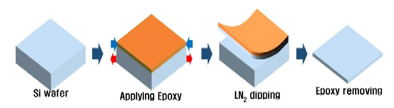
Bisphenol - A - (epichlorhydrin) translucent epoxy (MG Chemicals Company) was used as the SIL. Epoxy and resin (used as a hardener) were mixed at a 2:1 ratio and stirred by an impeller for 10 min. The Si mother wafer was cut to 5 cm × 5 cm and cleaned using piranha solution. After stirring the epoxy and resin, the resulting mixture was cured and uniformly applied to the Si mother wafer. After drying for 1 h, the sample was dipped into liquid nitrogen (LN2). The Si foil was lifted-off in LN2 and the epoxy was etched using piranha solution, as shown in Fig 1.
2.3. The Notch Creation by Laser Scribing
A notch was made by laser scribing to make the exfoliation of Si foil effortless and to control the crack propagation during the lift-off. As shown in Fig 2, the system is comprised of a UV laser source, beam delivery optics with a scanner device, a camera alignment detection part, control electronics, a loading stage, a safety part, and a control PC. The depth and position of the notch can be easily controlled by the laser power, line scribing number, and jig. The direct method for crack initiation is to create a notch on the top and the side of the substrate. Excellent performance, with narrow scribing lines and small holes of approximately 20 to 25 μm was achieved with the 355 nm (ultra-violet) wavelength laser beam. The Scanning Area was 170 × 170 mm2, and the maximum power was 10 watts. The depth of line at 1000X laser scribing was approximately 280 μm, and the depth of the line at maximum power was 3.4 μm, as shown in Fig 2.
2.4. Nickel Electroplating
The substrate of the Ti/Ni seed layer on the Si wafer was cut into a 10 cm × 10 cm square. Copper (Cu) tape (used as the electrode) was attached to the edges of the Si mother wafer and Kapton tape was attached to the substrate. Ni was electroplated onto a Ti/Ni seed layer, which was grown by evaporator. Sodium citrate tribasic dihydrate and nickel chloride hexahydrate were used to electroplate Ni onto the Si mother wafer. Nickel chloride (475.38 g) and sodium citrate (58.82 g) were mixed into the deionized water (DIW) 2L at 26 °C, and the pH was adjusted to approximately 3 to 3.5. The solution was stirred until the bubbles disappeared, for approximately 4 to 24. After stirring the solution for approximately 4 to 24 h, the substrate was dipped into the solution. The Ni was electroplated to the Si surface, excluding the area covered by Kapton tape. The solution was heated to 60 °C. Prior to electroplating, the contamination and oxide on the surface of the substrate were removed using a diluted hydrochloric acid to prevent the oxide layer from hindering the adhesion of Ni to Si on the substrate. After the pre-treatment of the substrate was completed, the substrate was dipped into the electroplating solution. The electroplating started after the current was set. The current was calculated by multiplying the electroplating area by the current density. The Ni electroplating was carried out using a current density of 8mA/cm2, an electroplating time of 2 h 50 min, a temperature of 60 °C, and a stirring speed of 150 rpm. After the Ni electroplating, the sample was dipped into the DIW. The electroplated Ni layer and Si foil were lifted-off from the Si mother wafer. After the lift-off, the electroplated Ni layer was etched with SC2 cleaning solution.
3. Results and Discussion
As shown in Fig 3, below 900 °C the Si was not exfoliated. However, Si was partially lifted-off at 950 °C. The lift-off of the Si foil was initiated by the difference in coefficient of thermal expansion (CTE) of the Si mother wafer and the Al SIL under rapid temperature change. The difference in the CTE of the Al paste and the Si is quite advantageous to the stress-induced lift off.
To improve the adhesion of the Al paste layer to the Si mother wafer and to prevent the Al paste layer from diffusing into the Si mother wafer, a SiNx layer was deposited using a plasma enhanced chemical vapor deposition (PECVD), to a thickness of approximately 60 nm. While the lift-off was only partially enabled by the Al paste layer as shown in Fig 3 (left), the Al paste layer and the SiNx enabled the lift-off entirely, as shown in Fig 3 (right). The Si foil thickness was measured to be approximately 58 to 69 μm; it was not uniform. Although the Al paste layer was enabled lift-off of the Si, the thickness of the Si foil was not uniform, and the Si foil was fragmented after etching the Al paste layer. Lift-off did not occur with a Al paste layer thickness of less than 60 μm or an annealing temperature below 950 °C.
The Al paste layer was approximately 50 μm thick per one screen printing, and the exfoliated Si layer was approximately 60 μm. As the Al paste layer thickness increased, the thickness of the exfoliated Si increased. After lift-off, 85% H3PO4 solution was used to remove the Al paste layer at 200 °C for 3 h 30 min. After being dipped into the H3PO4 solution, the Al paste layer and SiNx was removed, and the Si foil was fragmented. As a result, the Al paste layer and SiNx enabled the Si lift-off entirely on the 10 mm × 10 mm foil but the thickness of the Si foil was not uniform. After etching the Al paste layer, the Si foil was fragmented.
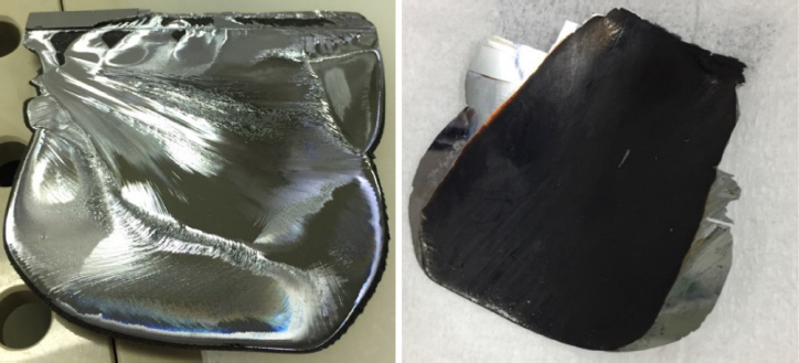
As shown in Fig 4, the epoxy layer with a notch on top were applied to the 5 cm × 5 cm substrate, and the Si foil was exfoliated. After the lift-off, the epoxy layer was etched using piranha solution. The Si foil was not uniform in thickness and was fragmented after etching the epoxy layer. In addition, the epoxy layer was not completely removed.
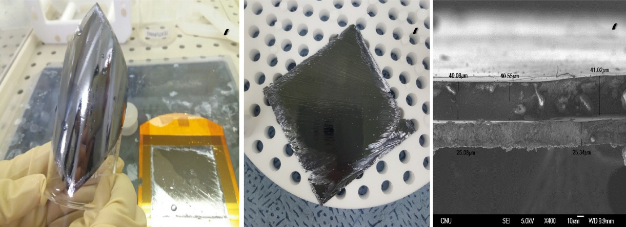
As shown in Fig 5, the Si foil was exfoliated by the electroplated Ni layer and was 10 cm × 10 cm in size. After the lift-off, the electroplated Ni layer was etched using an HCl and H2O2 solution; the Si foil thickness was approximately 40 μm. The spalled Si was uniform in thickness and the SIL was removed easily after the lift-off as compared to the Al paste layer and the epoxy layer.
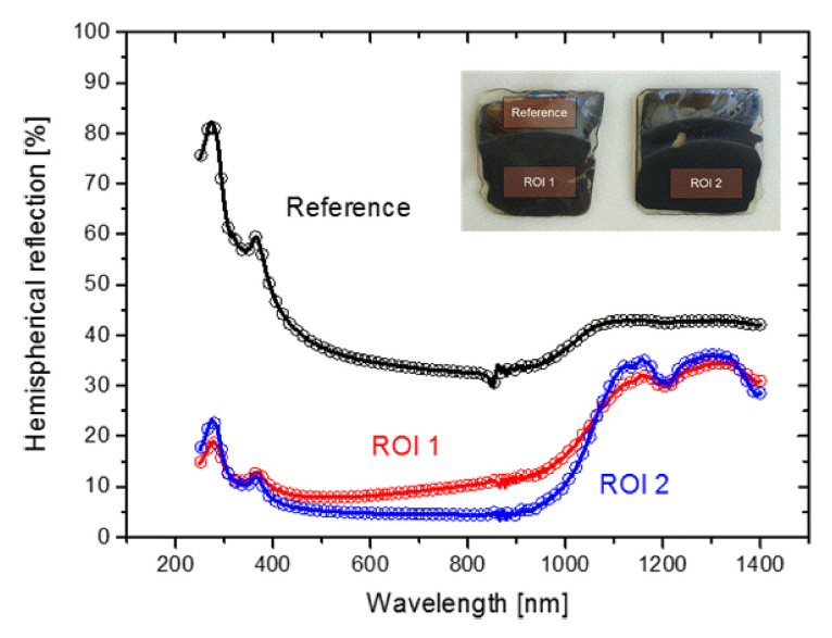
Thus far, the Al paste, epoxy, and electroplated Ni layer have been compared as the SIM and all three materials had the ability to induce Si lift-off. The Al paste was difficult to apply to a large area, and the Si foil was fragmented after the etching process. The epoxy layer exfoliated the Si foil with an area of 5 cm × 5 cm. However, the Si foil’s thickness was not uniform; it was also fragmented after the etching process. The Ni layer was electroplated onto a Ti/Ni seed layer, and the Si foil was exfoliated with an area of 10 cm × 10 cm and 40 µm thickness. As shown in Fig 6, after the inductively coupled plasma (ICP) texturing for the exfoliated Si wafer with the epoxy layer was completed, the reflection decreased to 3%, ranging approximately 400 to 1000 nm. The ICP texturing was conducted through international collaborative research at Fraunhofer-Center für Silizium Photovoltaik (CSP).
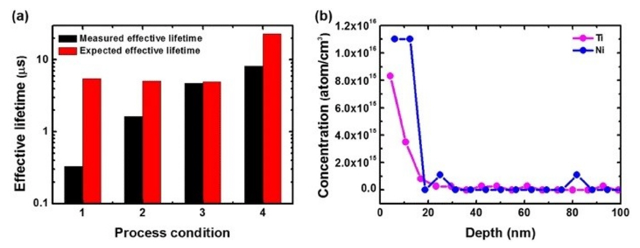
Fig 7 (a) shows that the minority carrier lifetime increased from process conditions 1 to 4. Process condition 1 was the spalled Si with a thickness of 50 µm, and its effective lifetime was 0.33 μs. Process condition 2 was the 4 µm etching of the fractured surface of the spalled Si wafer using a KOH solution before metal removal and the Al2O3 passivation. Its effective lifetime increased to 1.65 μs. Process condition 3 was approximately 500 nm etching using additional chemical etching and its effective lifetime was 4.71 μs. Process condition 4 was the post-annealing step of the Al2O3-passivated spalled Si after defect removal and its effective lifetime increased to 8.17 µs. Although the effective lifetime increased from process conditions 1 through 4, the measured effective lifetime was lower than the expected effective lifetime for each process conditions. It is possible that the slightly lower measured effective lifetime may have originated from a mechanical defect, Ti and Ni impurities (as shown in Fig 7 (b)), surface roughness, or the regeneration of micro/nano-cracks in the spalled thin Si wafers [18].
4. Conclusion
In this study, we investigated Si lift-off methods using Al paste, epoxy, and electroplated Ni layers. Although the Al paste layer and epoxy layers were successful for the lift-off of Si foil, the resulting exfoliated Si was not uniform and was easily fragmented after etching the SIL. Additionally, the Al paste layer and epoxy layers were difficult to apply to a large area. This study showed that the Al paste layer was completely removed but the epoxy layer was partially removed. However, the electroplated Ni layer expanded the spalled area to 100 mm × 100 mm. The thickness of spalled Si was uniform and the SIL layer of Ti/Ni was completely removed by etching solution. The spalled Si with a 50 µm thickness was passivated by Al2O3, and its lifetime was increased to 8.17 µs by the Al2O3 passivation and annealing process.