1. INTRODUCTION
Globally, environmental issues resulting from fossil fuels combustion and CO2 gas emissions have accelerated efforts to develop renewable energy sources. This interest in new types of energy sources is also important for IoT (internet of things) sensors and smart devices, which could potentially benefit from energy harvesting. Energy harvesting is the process of recovering ambient energy and converting it into electricity. Among energy harvesting technologies, thermoelectric systems are popular because they can directly convert heat into electricity. Waste heat can be retrieved virtually from any source, including vehicles, electronic devices, and even human bodies. The efficiency of a thermoelectric material is described by a dimensionless figure of merit (ZT). Efficient thermoelectric materials require a large power factor and low thermal conductivity at application temperatures.
In the continuing search for eco-friendly thermoelectric materials comprising non-toxic and low-cost elements, Cu-Sb-S compounds such as Cu3SbS4 (famatinite), Cu12Sb4S13 (tetrahedrite), Cu3SbS3 (skinnerite), and Cu3SbS2 (chalcostibite) have attracted attention as p-type thermoelectric materials. The aforementioned compounds, except Cu3SbS4, have a low thermal conductivity because of their anharmonic lattice, which is caused by electrostatic repulsion between Sb 5s lone-pair electrons and neighboring atoms. Among these compounds, Cu3SbS3 has the largest SŌĆōSbŌĆōS bond angle, which is responsible for its low lattice thermal conductivity [1]. In addition, Cu3SbS3 has been reported to be a promising photovoltaic material because of its ideal bandgap energy (1.40ŌĆō1.84 eV) and high absorption coefficient [2-5]. However, studies on its thermoelectric performance are limited.
Cu3SbS3 also has three temperature-dependent crystal structures [6,7]: orthorhombic (space group P212121, < 263 K), monoclinic (space group P21/c, 263ŌĆō395 K), and orthorhombic (space group Pnma, > 395 K) structures. The Cu atoms move from ordered sites to disordered sites with increasing temperature. Recently, Cu3SbS3 with a cubic structure (space group I4 ┬»
Generally, synthesizing chalcogenides using a melting method requires slow heating/cooling rates because of the high vapor pressure and low boiling point of the chalcogen elements, and their lengthy annealing for homogenization [11-13]. In our previous studies [14-16], Cu-based chalcogenides were successfully synthesized by a relatively fast MA method without subsequent heat treatments. MA is a solid-state process involving repeated fracturing and cold welding between elemental powders and steel (or tungsten carbide or zirconia) balls, and has the advantage of avoiding the volatilization and segregation of chalcogen elements which typically occurs in the melting process [17]. It is also a cost-effective method because it consumes less energy and time. In this study, Cu3SbS3 bulk specimens were prepared by the solid-state MA-hot pressing (HP) synthesis process, and the effects of MA-HP conditions (MA time and HP temperature) on their phase synthesis (transformation) and thermoelectric properties were examined.
2. EXPERIMENTAL PROCEDURE
The chemicals required for the synthesis of skinnerite Cu3SbS3, Cu (purity 99.9%, < 45 ╬╝m), Sb (purity 99.999%, < 75 ╬╝m), and S (purity 99.99%, < 75 ╬╝m) elemental powders were weighed in stoichiometric ratio, and loaded into a hardened steel jar with steel balls. Planetary ball milling (Pulverisette5, Fritsch) was performed for MA at 350 rpm for 6ŌĆō24 h in an Ar atmosphere. The MA powders were hot-pressed in cylindrical graphite at 523ŌĆō623 K for 2 h under a uniaxial pressure of 70 MPa in a vacuum.
The phases of the MA powders and HP compacts were identified by X-ray diffraction (XRD; D2-Phaser, Bruker) with Cu K╬▒ radiation. Rietveld refinement (TOPAS, Bruker) was performed to obtain crystallographic information and estimate the lattice constants. The weight variations and phase transformations of the MA powders and HP compacts were analyzed by thermogravimetry and differential scanning calorimetry (TG-DSC; TG/DSC1, Mettler Toledo), in which the temperature was increased to 973 K at a heating rate of 5 Kmin-1 in an Ar atmosphere. The microstructure was observed and elemental compositions were analyzed by fielde-mission scanning electron microscopy (FESEM; JSM-7610F, JEOL) in conjunction with energy-dispersive spectroscopy (EDS; X-Max50, Oxford).
The Hall coefficient was measured using the van der Pauw method (7065, Keithley), and then the carrier concentration and mobility were evaluated by assuming that the electrical conditions are dominated by a single charge carrier. The electrical conductivity (Žā) and Seebeck coefficient (╬▒) were measured using the DC four-probe method using ZEM-3 (Advance Riko) equipment in a He atmosphere. The thermal diffusivity (D) was measured using the laser flash method with a TC-9000H (Advance Riko) system in vacuum. Then, the thermal conductivity (╬║ = Dcpd) was estimated from the thermal diffusivity, specific heat (cp), and density (d). The thermoelectric power factor and figure of merit were evaluated at temperatures in the range of 323ŌĆō623 K.
3. RESULTS AND DISCUSSION
Figure 1 shows the XRD patterns of the Cu3SbS3 specimens. The cubic Cu3SbS3 (I4 ¯
Figure 1(b) shows the XRD patterns of the sintered specimens at different HP temperatures. The cubic Cu3SbS3 phase in the MA powder remained even after HP; however, a secondary phase of Cu2S was identified when it was hot-pressed at 673 K (HP673K2H). Du et al. [8] reported that many types of Cu2-xS phases were produced, when cubic Cu3SbS3 was synthesized by the MA-SPS process, and they could not obtain a single cubic Cu3SbS3 phase without a suitable dopant.
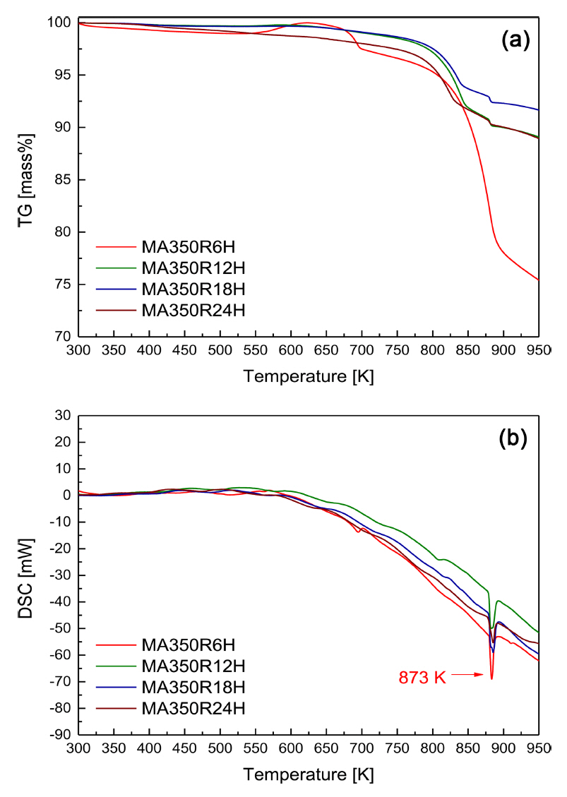
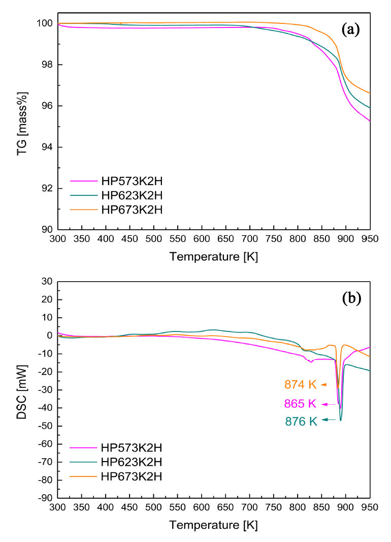
The TG-DSC curves of the hot-pressed Cu3SbS3 specimens are shown in Fig 3. The DSC curves of the HP specimens exhibited small endothermic peaks at 798ŌĆō808 K and large endothermic peaks at 865ŌĆō876 K. Skinner et al. [18] reported that tetrahedrite (Cu12Sb4S13) + chalcostibite (Cu-SbS2) were transformed into famatinite (Cu3SbS4) + skinnerite (Cu3SbS3) at 795 ┬▒ 2 K, and then chalcostibite + Sb were transformed into skinnerite + liquid at 804 ┬▒ 2 K. Because the melting point of Cu2S is 1143 K [19], its reaction peaks did not appear in the measured temperature range in the present study. Therefore, as indicated in Fig 2, the large endothermic peaks were attributed to the melting point of Cu3SbS3, and the small endothermic peaks were possibly due to phase transformation by sulfur volatilization.
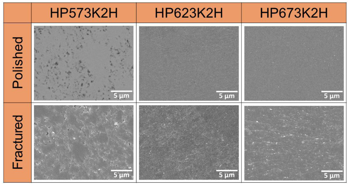
Figure 4 displays FESEM images of the polished (backscattered electron mode) and fractured (normal mode) surfaces of HP Cu3SbS3. Considering HP573K2H (the specimen hot-pressed at 537 K for 2 h), a microstructure with many pores and low density was observed, which was consistent with the low relative density in Table 1. However, HP623K2H and HP673K2H had no pores or cracks, and their relative densities were more than 99% of the theoretical density (5.1 g cmŌłÆ3) [20]. The Cu2S phase detected in the XRD patterns for HP673K2H could not be observed in the surface image.
The nominal and actual compositions of the Cu3SbS3 are presented in Table 1. The actual composition of the MA powder was similar to the nominal composition; however, the actual composition of the HP specimens was slightly different than the nominal composition, which was predominantly due to the volatilization of high vapor pressure Sb and S atoms during the sintering process. The lattice constant of the MA powder was 1.0343 nm, and it increased with increasing HP temperature, to a final range of 1.0365ŌĆō1.0394 nm. Machatschkj [21] reported the lattice constant of cubic Cu3SbS3 to be 1.0320 nm, and Du et al. [8] reported lattice constants of 1.0391 (before heat treatment) and 1.0343 nm (after heat treatment) for the Fe-stabilized cubic Cu3Fe0.1Sb0.9S3 prepared by MA-SPS. Nefzi et al. [4] synthesized the orthorhombic Cu3SbS3 phase via direct fusion and obtained lattice constants of a = 1.0247 nm, b = 1.3253 nm, and c = 0.7846 nm. The lattice constants of monoclinic Cu3SbS3 have been reported to be a = 0.7814 nm, b = 1.0242 nm, and c = 1.3273 nm [22].
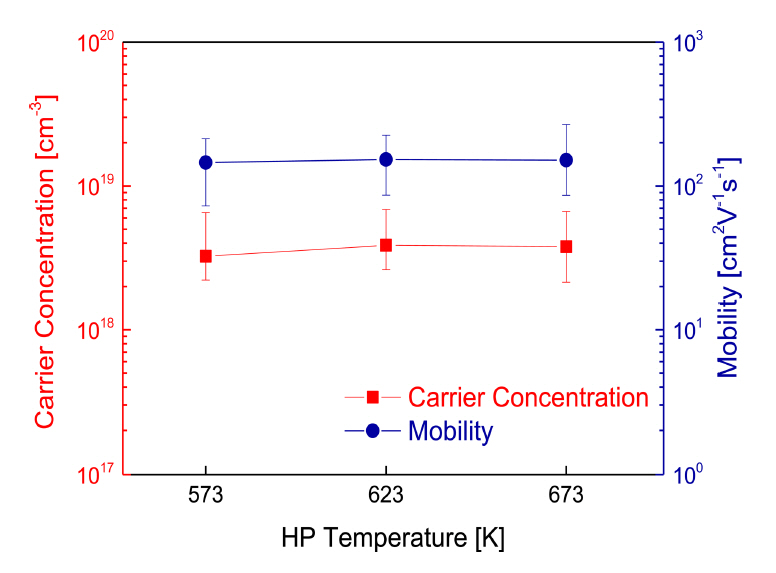
Figure 5 presents the charge transport properties of Cu3SbS3 at different HP temperatures. All of the skinnerite compounds were found to be p-type semiconductors with hole concentrations of (3.25ŌĆō3.87) ├Ś 1018 cmŌłÆ3 and carrier mobility of 146ŌĆō153 cm2 VŌłÆ1sŌłÆ1. In Cu chalcogenide compounds, Cu vacancies with low formation energies are easily formed and contribute to p-type behavior [23]. A high carrier concentration of 9.1 ├Ś 1019 cmŌłÆ3 and low mobility of 3.7 cm2 VŌłÆ1sŌłÆ1 were reported for cubic Cu3SbS3 prepared by MA-SPS [8]. The carrier scattering was increased because the fine grain size of the sample was maintained by the SPS method, due to the short sintering time compared with HP, resulting in lower carrier mobility.
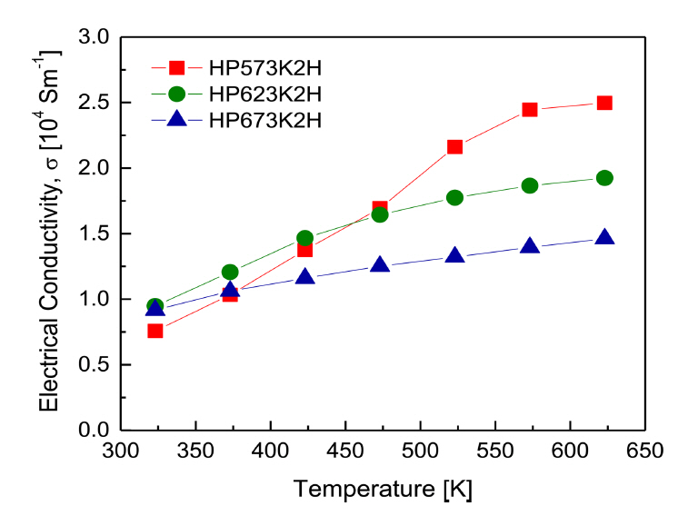
Figure 6 shows the electrical conductivity of Cu3SbS3 at different HP temperatures. The electrical conductivity increased with increasing temperature, indicating nondegenerate semiconductor behavior, and the electrical conductivity at high temperatures decreased with an increase in HP temperature. A high sintering temperature might cause a small discrepancy in the composition, which could decrease the carrier concentration [24]. Therefore, the decrease in electrical conductivity with increasing HP temperature could be attributed to the change in the carrier concentration, because of the volatilization of sulfur with high vapor pressure. Chen et al. [1] reported that Cu3SbS3 prepared by MA-SPS (at 623 K for 3 min) had a low electrical conductivity of approximately 10 S mŌłÆ1 because of its intrinsically low carrier concentration. Du et al. [8] obtained an electrical conductivity of 540 S mŌłÆ1 at room temperature for Cu3SbS3 prepared by MA-SPS (at 673 K for 5 min). In this study, the electrical conductivities of Cu3SbS3 at 323 and 623 K were (7.6ŌĆō9.5) ├Ś 103 S mŌłÆ1 and (1.5ŌĆō2.5) ├Ś 103 S mŌłÆ1, respectively. These high values could be attributed to the increased carrier mobility that resulted from grain growth during the HP process, because of its slower heating/cooling rate and longer holding time (at 523ŌĆō623 K for 2 h) compared with SPS.
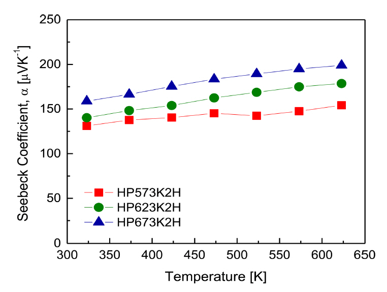
Figure 7 presents the Seebeck coefficient for Cu3SbS3 at different HP temperatures. The Seebeck coefficient values were positive, indicating p-type conduction in accordance with the signs of the Hall coefficient. Generally, as the temperature increases, the Seebeck coefficient increases and then decreases after reaching a maximum value because of intrinsic conduction induced by thermal excitation. In this study, the Seebeck coefficient of Cu3SbS3 continued to increase as the temperature increased, and intrinsic conduction did not occur in the temperature range of 323ŌĆō 623 K. According to the Pisarenko relation, as the carrier concentration decreases, the Seebeck coefficient increases. Therefore, the increase in the Seebeck coefficient with an increase in HP temperature was due to the reduction in carrier concentration. The power factor (PF = ╬▒2Žā) calculated from the Seebeck coefficient and electrical conductivity is presented in Fig 8. As the temperature increased, the power factor of all specimens increased, and the maximum PF was 0.58ŌĆō0.61 mW mŌłÆ1 KŌłÆ2 at 623 K.
Figure 9 shows the thermal conductivity of Cu3SbS3 at different HP temperatures. The thermal conductivity consists of the lattice thermal conductivity (╬║L) from the lattice vibrations and the electronic thermal conductivity (╬║E) from the charge carrier transport. This can be separated using the Wiedemann-Franz law (╬║E = LŽāT), where the Lorenz number (L) can be obtained using the equation L [10ŌłÆ8 V2 KŌłÆ2] = 1.5 + exp(ŌłÆ|╬▒|/116) [25]. In this study, the Lorenz number ranged from (1.75ŌĆō1.82) 10ŌłÆ8 V2 KŌłÆ2 at 323 K to (1.68ŌĆō1.76) ├Ś 10ŌłÆ8 V2 KŌłÆ2 at 623 K. These results suggest that Cu3SbS3 is a nondegenerate semiconductor. Theoretically, the Lorenz number is in the range of (1.45ŌĆō2.44) ├Ś 10ŌłÆ8 V2 KŌłÆ2 [26]; a smaller value indicates nondegenerate semiconductor behavior, and a larger value indicates degenerate semiconductor (or metallic) behavior.
The thermal conductivities of all the specimens were lower than 0.78 W mŌłÆ1 KŌłÆ1 in the temperature range of 323ŌĆō623 K. An increase in electrical conductivity led to an increase in electronic thermal conductivity with increasing temperature; however, the lattice thermal conductivity was almost temperature-independent. Skoug et al. [27] reported that electrostatic repulsion between the Sb 5s lone-pair electrons and neighboring chalcogen ions created an anharmonicity in the lattice; its strength was determined by the XŌĆōSbŌĆōX (X: chalcogen atom) bond angle and the coordination number of the group AV atom. Accordingly, Cu3SbS3 with the largest SŌĆōSbŌĆōS bond angle (99.3) exhibited the lowest lattice thermal conductivity and temperature-independent behavior.
Figure 10 shows the ZT (= ╬▒2Žā╬║-1T) of Cu3SbS3. As the temperature increased, the ZT values of all the specimens increased, reaching a maximum ZT value of 0.57 at 623 K. This was significantly higher than the ZT Ōēł 0.01 at 623 K for orthorhombic Cu3SbS3 prepared by MA-SPS [1] and ZT Ōēł 0.2 at 625 K for cubic Cu3SbS3 [8], mainly owing to the high electrical conductivity and PF. The cubic skinnerite Cu3SbS3 prepared by MA-HP in this study could be a potential thermoelectric material, as its thermoelectric performance can be enhanced by stabilizing the phase and optimizing the carrier concentration via doping.
4. CONCLUSIONS
Cubic skinnerite Cu3SbS3 was successfully synthesized using the MA-HP solid-state process. From the XRD phase and TG-DSC thermal analyses, the optimal MA conditions were determined to be 350 rpm for 18 h. Compacts close to the theoretical density were obtained under HP temperature conditions of 623 K or higher. All the specimens behaved like p-type nondegenerate semiconductors. As the HP temperature increased, the electrical conductivity decreased because the carrier concentration decreased, due to the volatilization of sulfur; however, the Seebeck coefficient increased. All the specimens had thermal conductivities lower than 0.78 W mŌłÆ1 KŌłÆ1. The specimens hot-pressed at 623 and 673 K exhibited power factors of 0.61 and 0.58 mW mŌłÆ1 KŌłÆ2 and ZT values of 0.51 and 0.57, respectively. The MA-HP process was confirmed to be a practical method for the solid-state synthesis and sintering of cubic Cu3SbS3, which could be a potential thermoelectric material.


