Transition Metal Dichalcogenide WS2 Films Prepared with a Combination of Spin/Dip Coating and CVD
Article information
Abstract
Recently, transition metal dichalcogenides (TMDCs) with 2D structure have attracted interest due to their many unique optical and electrical properties. The primary preparation methods for 2D materials are chemical vapor deposition (CVD), exfoliation, and other vacuum technologies. Large-scale synthesis of WS2 via solution-process is rare due to the higher temperature needed for tungsten-based precursors. Combination of spin coating or dip coating with CVD have been studied recently to make large-area 2D TMDC with good electrical properties. Here, we report a new synthetic route for large WS2 crystal that combined solution coatings and CVD process. A solution of sodium tungstate and hydrazine hydrate with sodium thiosulphate was coated on a silicon wafer via dip and spin coating. The films were then treated with CVD at various positions and temperatures to facilitate crystallization. The double coating conditions and CVD parameters were modified to obtain WS2 crystals. Triangular shaped 44 ± 4 µm WS2 crystals could be obtained with simple annealing above 900°C without gas treatment. The synthesized WS2 was found to be bulk with a triangular shape, as confirmed by Raman and AFM analyses. A PL peak of WS2 at 643 nm was observed at an early crystallization stage.
1. INTRODUCTION
Even though graphene has many potential uses, including electrical, optical, and biomedical applications, the practical realization of graphene seems limited by its band gap of zero. Recently, in the field of nanoelectronics and optoelectronics, two-dimensional (2D) transition metal dichalcogenides (TMDC), which are analogous to graphene, have attracted considerable attention because of their electrical and innate band gap characteristics. These can be divided into semiconductor, semimetal, and metal characteristics because of the coordination of TMDCs.
Among them, MoS2 and WS2 show particular interesting properties. They have a direct and indirect band gap of 1.8 eV and 1.2 eV, respectively, depending on the monolayer stacking states. Thin layered WS2 composed of a S-W-S crystalline sandwich with a van der Waals bonding, possess the coupled spin and valley physics [1], and high photoluminescence efficiency [2]. It can also be used in composited layered materials with other 2D materials for many applications [3]. Most studies on 2D TMDC have been focused on their chemical synthesis using chemical vapor deposition (CVD), and by mechanical methods like exfoliating flakes by tape or in liquid.
In order to make large-area and high-quality 2D TMDC with good electrical properties, various spin coating or dip coating methods combined with CVD methods have been intensively studied in the last few years. High thermal annealing of thermally decomposed ammonium thiomolybdate with sulfur resulted in highly crystalline MoS2 after dip coating [4]. A bottom gate transistor with synthesized MoS2 was demonstrated and showed electron mobility comparable to that of micromechanically exfoliated MoS2 nano-sheets. The highly controllable thickness of MoS2 thin film grown via a spin-coating route resulted in wafer-scale homogeneity with crystalline and stoichiometric chemical composition [5]. Our group reported a new solution synthesis route for MoS2 films with one step annealing without CVD for the first time [6]. New electrohydrodynamic jet patterned MoS2 films were reported from precursor solution with one step annealing [7]. More recently, deionized (DI) water-based solution processed MoS2 was also reported [8].
However, the CVD method for WS2 crystal layers is more challenging than MoS2 because of the higher temperature needed for tungsten-based precursors. In some case, WS2 bulk powder can be formed by the direct reaction of sulfur with the bulk WO3, which stops the growth of the domains of WS2 . Therefore, two furnace systems were used in CVD to accurately control the time for introducing sulfur to make large WS2 domains [9]. It is not possible to obtain large WS2 from mechanical exfoliation due to the difficulty in taking a crystalline layer from a clump.
WS2 was also obtained by the evaporation of WO3 by hydrogenation and sulfurization in CVD with H2 and Ar under low pressure [10]. Controlling H2 concentration was crucial to obtain large crystals. Using ambient pressure during the CVD, large single-crystal WS2 was prepared on Au foil by a surface growth mechanism. It could be transferred to any substrates, without wrinkles or damage by using an electrochemical bubbling technique. However, an expensive Au substrate was used because it does not react with sulfur, and acts as a catalyst to lower the reaction energy [11].
Large-scale synthesis of WS2 via solution-process is rare. WS2 nanosheets with a lateral dimension of 100 nm were prepared from 1D W18O49 with surfactants and a rolling-out method, A powder of WS2 nano-sheet was prepared by a two-step method of ball-milling and thermal annealing. A hydrothermal reaction was employed to obtain a 2D nano-sheet, but it was not easy to obtain a 2D form because WOx prefers 1D or 0D formation, in contrast to MoS2 [12]. Recently, the facile fabrication of WS2 was demonstrated using a thermal decomposition of precursor with two annealing processes. The first annealing step was used to achieve the lateral epitaxial growth of the WS2 and the second annealing was in S-rich and high-temperature conditions [13]. Atomically thin WS2 from a solution process was reported using CVD under H2 gas, and it was applied to optoelectronic devices [14]
We have prepared a new synthesis route by combining solution coating and a CVD process. In order to obtain a uniform and large size WS2 crystal, a solution of sodium tungstate and hydrazine hydrate with sodium thiosulphate was coated on a silicon wafer with controlled parameters via two coating methods; dip coating and spin coating. The coated wafer was thermally treated with CVD using sulfur with different positions and temperatures to investigate the crystalline formation. Large-scale WS2 crystals with triangular shape could be obtained.
2. EXPERIMENTAL
The precursor solution was prepared as follows, 5 mL of (0.25 M) sodium tungstate in hydrazine hydrate, 2.5 mL of (0.1 M) citric acid, and 10 mL of (0.25 M) sodium thiosulphate were added to 50 mL of DI water. P-type Si wafer with a thermally-grown 300 nm layer of SiO2 was cleaned with IPA, acetone and DI water. The wafer was treated with UV/O3 for 10 min to improve surface wettability and obtained better film coverage. After the precursor solution was heated to 70°C in an oil bath, the silicon wafer substrate was dipped into the precursor solution for 1h 30 min to coat it. After it was removed from the solution, the substrate was spin-coated with the precursor solution at 2000 rpm for 30 s.
After soft baking the substrate at 150°C for 15 min, the sample was treated by CVD with sulfur powder and annealed for 30 min under N2 flow at various positions at temperatures of 600°C to 1000°C. The sample positions were 25 cm, 35 cm, and 40 cm from the inlet, and the sulfur was positioned at 5 cm from the inlet. The temperature and relative humility were controlled to keep the evaporation conditions stable during the experiment. Raman spectra and PL were collected with a confocal Raman spectrometer (LabRAM HR800) using a 532-nm laser as an excitation source. The laser spot size was approximately 1 µm at 60 µW.
3. RESULTS AND DISCUSSION
To prepare a suitable solution for the WS2 precursor, several compounds were tested, and sodium tungstate was chosen. A solution formulation was developed with a mixture of hydrazine and sodium thiosulfate in DI water. However, solid film could not be formed on the substrate by dip coating with the solution formulation. With spin coating, the precursor film was not uniformly formed even after surface treatment of the substrate with UV/O3. The combination of dip and spin coating was employed to obtain better films. To create some seed layers, an initial dip coating was performed. Spin-coating could then be performed on the seeded layer to obtain uniformly coated films. These two coating steps provided solid films on wafer.
Thermal treatment is then required to promote crystal growth from the wet precursor films. To make WS2 crystals, the double-coated layer was inserted into a reactive furnace with sulfur powder, as shown in Fig 1. The effect of furnace temperature on the crystal growth was investigated. Interestingly, the formation of WS2 films started from 600°C. Perfect crystals were formed at 900°C and 1000°C, but, the crystals also started growing at much lower temperatures, as shown in Fig 1b-e. When annealed, the chamber was maintained at a low pressure of 35 Torr with a nitrogen flow of 5.2 sccm for 30 min for inert conditions.

(a) Distance of the samples from the inlet in CVD, P1; 25 cm, P2; 35 cm, P3; 40 cm, and S; sulfur (rotary, RP, and diffusion, DF, pump systems). (b-e) OM images of WS2 at (b) 1000, (c) 900, (d) 800, and (e) 600°C of annealing temperatures
The amount of sulfur was another factor to control. Sulfur was placed at 5, 8, and 11 cm from the inlet of the furnace. When the sulfur was placed at a distance of 5 cm, the WS2 crystals had a normal shape with broad distribution. However, when the distance was increased to 8 and 11 cm, the WS2 crystal shape was changed, and relatively uneven crystals were observed. Therefore, the distance was fixed at 5 cm with different annealing temperatures (600, 700, 800, 900, and 1,000°C).
The sample position was varied to 25, 30, and 40 cm from the furnace inlet, as shown in Fig 1a. The size distribution of WS2 varied with not only sulfur position, but also sample positions. The average size was around 44 ± 4 µm for a position 25 cm from the inlet. It was around 40 ± 5 µm for 30 cm and around 32 ± 6 µm for 40 cm position, as shown in Fig 1b. It is not easy to draw conclusions about the dependence of sample position and crystal size. The farthest position from the inlet, 40 cm, showed a relatively broad distribution of crystal, and random shapes of crystals were observed. In general, a position closer to the inlet led to relatively large crystal size and even size distributions. This was because the sulfur powder was more easily accessible, which it was closer to the precursor-coated sample.
When the temperature was lower than 900°C, crystal growth was different, depending on the sample position. For example, at 800°C, the crystal growth was incompletely finished due to the low annealing temperature. At 30 cm and 40 cm, triangle-shaped crystals of WS2 were observed with star-shape and rectangular crystals. These incomplete crystal growths were due to the annealing temperature, which was not high enough, and the lower availability of sulfur powder due to the long traveling distance. When the annealing temperature was 600°C, a few crystalized triangular crystals were observed, but there were many under-crystalized domains, like islands on the sea, as shown in Fig 1e. When the annealing temperature was over 900°C, all WS2 were crystalized into triangular shapes, regardless of the positions. The triangular shaped WS2 with multi apex is attributed to the growth rate of the W and S.
The effect of annealing temperature can be clearly understood from the OM images of WS2 crystals with temperatures, as shown in Fig 1b-e. In general, a higher thermolysis temperature leads to higher crystallinity in the WS2 film. At 900 and 1000°C, WS2 crystals were obtained with a relatively large size and even distribution. A WS2 crystal size of around 44 µm was obtained at the annealing temperature of 1000°C. However, at 800°C, the crystal size was reduced because there was insufficient crystallization. Premature crystal shapes were observed at 600°C.
We confirmed that relatively large size 42 - 48 µm of WS2 crystal could be obtained with the double coating. In the literature, when two furnaces in separate systems were used to control the sulfur, mostly small sizes of WS2 were reported [9]. With another CVD method with WO3, no WS2 could be formed without H2 gas, and WS2 crystals were observed under H2/Ar gas mixture [10]. However, we obtained large WS2 crystals through simple annealing without H2 gas.
Raman spectra can be used to characterize the synthesized WS2 films, as shown in Fig 2. The in-plane optical mode of E12g for WS2 appears at approximately 350 cm-1. The out-of-plane vibration of sulfur of A1g appears at 421 cm-1. As seen in Fig 2a, the different sample positions in the furnace affects the peak intensity of the Raman spectra. A similar effect on crystal sizes was mentioned above. The closest position, P1 (25 cm from inlet of furnace), showed the highest peak among the positions. Compared with another WS2 synthesis method, Raman peaks showed E12g at 355-358 cm-1 and A1g at 417-419 cm-1 depending on the synthesis methods. The double coating methods shows a lower E12g and higher A1g, and a larger a difference for different positions.
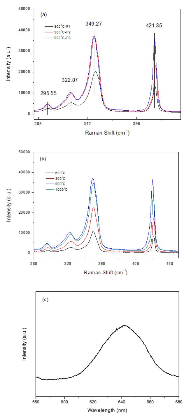
(a) Raman spectra of synthesized WS2 with different sample positions in CVD, (b) Raman spectra of WS2 at various annealing temperatures. (c) PL spectrum of synthesized WS2 showed at 643 nm.
In general, the position of these two peaks and their difference provide information on the number of layers in the crystals. When the frequency difference is around 60 to 64 cm-1, WS2 will have 1 to 5 layers. Above this, the samples are classified as bulk materials. Therefore, from the difference in the two peaks at 71 cm-1, the films from our solution method can be considered bulk.
It is hard to identify these multi-phonon bands in the two other peaks of WS2 that appear at 295 and 322 cm-1 (Fig 2a), which may be assigned as the combination modes of 2LA-2E22g, and 2LA-E22g [13] or 2ZA(M) and LA(M)+TA(M) [15]. Charting th Raman spectra with annealing temperatures to show the intensity of the peaks with temperatures, the higher peaks appear with higher temperatures. The same trend and peaks can be observed at the lowest temperature of 600°C. Interestingly, the Raman peaks for sample temperature above 900°C show that the sample closest to the inlet had the highest peak intensity, which can also be confirmed from Fig 2b.
The triangular crystals and the thickness are clearly demonstrated in AFM measurements, as shown in Fig 3. The AFM image shows an approximately 125-nm thickness with 3.2-nm roughness at 800°C and 200-nm thickness with 6.2-nm roughness at 1000°C. The WS2 films are relatively thick layers, which may be the result of the double coating methods. A relatively thick layer is formed due to the dip coating to make a seed layer on the substrate. We found that it was not possible to make a film by simple spin coating only. Dip coating is also critical for film formation, and seed molecules from the dip coating keep the precursor solution on the substrate during spin coating and increase nucleation density.

AFM images and thickness profiles of WS2 at annealing temperature of 800 and 1000°C.
Even though a spin coating technology is available using diluted (NH4)2WS4 solution, H2 gas is needed to protect the effect of oxygen on the crystallization of WS2 films during annealing [13, 14]. WS2 has also been obtained by the reduction and sulfurization of WO3 with high H2 concentration [10]. Even though mono- to multi-layers of WS2 could not be obtained, unlike other studies no gas was used during our process. And we obtained relatively large sized triangular WS2 crystals on wafer, which are suitable for potential applications.
The WS2 monolayer showed strong PL emission with strong spin-orbital coupling. The PL peaks for mono- and bilayers were reported to be 641 nm with a sharp and narrow FWHM [10]. In general, PL peaks are rarely observed in multi-layer WS2 because of the change from a direct to an indirect band gap [16]. The triangular shaped WS2 showed a broad PL spectrum at 643 nm at 700°C, as shown in Fig 2c. The reason might be that mono- or few-layer WS2 could have formed during an early stage of crystallization annealing. After crystallization, no peak was observed due to the multi or bulk crystals.
4. CONCLUSIONS
To obtain large WS2 crystals from solution synthesis, a combined dip and spin coating method with CVD was developed. The effect of sample position and sulfur during CVD was investigated with a focus on the crystal size and distribution of WS2. The sample position of 25 cm from the CVD inlet and 5 cm from the sulfur source were suitable to obtain triangular crystals. Even though the annealing temperature is crucial for crystallization, WS2 starts to form crystal at the relatively low temperature of 600°C, with complete crystallization above 900°C. The relatively large size of around 44 ± 4 µm WS2 could be obtained from the solution method by simple annealing without gas treatment. The resulting WS2 was found to be a bulk material using the double coating method, as confirmed by Raman and AFM. Interestingly, a broad PL peak was obtained from the WS2 film prepared at 700°C. This might be the early stage of crystal formation before growing into bulk material. Further work is necessary to control the atomic layers of WS2 for optoelectronic applications.
Acknowledgements
This work was supported by the Basic Science Research Program through the National Research Foundation Korea (NRF-2018R1D1A1B07048441) and Regional Innovation Strategy (RIS) through the NRF funded by the Ministry of Education (MOE, 2021RIS-004).
Notes
Competing interests
The authors declare no competing interests.