Interfacial Layer Effect on the Adhesion of the Ultra-Hard Thick TAC Film Deposition
Article information
Abstract
Carbon-based thin film tool coatings, such as diamond-like carbon (DLC), have excellent lowfriction and anti-sticking properties. These thin films are widely used for the cutting and machining of increasingly widely-used lightweight non-metallic and non-ferrous metal materials, as a part of countermeasures against global warming. However, non-metallic and non-ferrous metal materials are significantly inferior in strength and heat resistance compared to iron-based metals. Therefore, they are primarily employed in high-content fiber reinforced composite materials, which significantly improves their mechanical and thermal properties. Tetrahedral amorphous carbon (TAC) coating has a hardness level similar to diamond coating. However, when TAC is deposited as a thick film, delamination of the coating layer may occur because of the high internal compressive stress between the carbide-based substrate and coating layer, thereby restricting its scalability to other applications. Other factors to be controlled for thick film TAC deposition include minimizing droplets generated during the coating process, and improving interfacial properties like hardness and fatigue resistance. Here, C in the form of CH4, which has high solubility over Cr and forms various compounds, was added during the interfacial deposition process, between the carbide and TAC, to improve interfacial strength and adhesion by precipitation of carbide at the interface. This eventually led to thick TAC film with the thickness and adhesion of commercially viable thick film.
1. INTRODUCTION
Excessive emissions of CO2 gas from the increased consumption of carbon-based fuels is resulting in severe air pollution, destruction of the ecosystem, and global warming, which are threats to human survival. Along with efforts to develop alternative fuels as one of another countermeasures, it is the introduction of polymer composite materials, such as carbon-fiber-reinforced polymers (CFRP) and glass- fiber- reinforced polymers (GFRP), are widely used as aircraft materials because of their high specific strength. They can also reduce the weight of vehicles and other transportation systems.In addition, metal matrix composite (MMC), ceramic matrix composite (CMC), and non-ferrous metal materials (e.g., Al, Mg, Ti) are increasingly used in the aerospace industry in the form of alloys or composite materials, which can reduce vehicle weight by 50–70% [1-3].
Recently, the aerospace industry has rapidly increased the use of hybrid composite-metal stack materials, in which a resin-based composite material, such as CFRP, and a metal, such as Al or Ti, are bonded to each other. Stack materials can simultaneously improve weight, specific strength, and heat resistance [4].
These fiber-reinforced composite, non-ferrous, and non-metallic materials require high-speed cutting in a dry environment to reduce costs and improve productivity. For this purpose, a diamond-like carbon (DLC) coating with high hardness and low friction is primarily applied on tool surfaces [5,6]. Tetrahedral amorphous carbon (TAC), which does not have hydrogen, exhibits an ultra-high hardness of 4,000–8,000 HV, similar to that of a diamond coating. The diamond coating is fabricated using hot filament chemical vapor deposition (HFCVD) technology, and exhibits a hardness of 4,000–10,000 HV. Even though HFCVD diamond and TAC coatings have similar levels of hardness, the TAC coating can be widely used in the tool industry. There are practically no restrictions on material type or shape, and it has excellent surface roughness, sharp edge maintenance, and low production cost.
However, because of the high hardness of the coating layer, high internal compressive stress develops from internal defects that result from the combined deposition of droplets when deposited as a thick film. When there is a significant difference between the hardness of the coating layer and the matrix material, flaking of the coating layer can occur during cutting operations, as increasing fatigue accumulates at the interface of both materials [7,8].
Several studies have been conducted on the deposition of thick thick TAC film to obtain properties comparable to those of HFCVD diamond-coated tungsten carbide tools (WC-Co). A few improvements in properties, such as the hardness and thickness of the coating layer, and tool shape, have been demonstrated; however, several limitations still remain unsolved [8,9].
Recently, expectations and possibilities for TAC thick film deposition have started rising again because of the development of facilities that can precisely control droplets, and enable high-speed deposition with high output, even at low-temperature. However, to deposit a thick coating of ultra-hard TAC, further studies need to be performed to determine the interfacial bonding force between the high-hardness matrix material, such as tungsten carbide, and the ultra-hard thick TAC film, similar to that of HFCVD diamond.
Cr and Ti are representative materials that can be used as an interlayer to strengthen the bonding force at the interface between carbide (2,000 HV) and TAC (5,000 HV). The Cr layer, deposited by physical vapor deposition (PVD), has a high hardness of 900–1,200 HV. The melting point of this layer decreases significantly with increasing C contents, and various carbides (Cr23C6, Cr7C3, Cr3C2) can be generated through temperature control (Fig 1a). In contrast, the Ti layer, deposited by PVD, has a hardness of 200–500 HV, which is significantly lower than that of Cr. The melting point increases with increasing C contents and the formation of carbide is extremely difficult (Fig 1b) [10–12].

Table 1 lists the types, crystal structures, and hardness of carbides which can be produced by the reaction of Cr and C. Data for WC-Co-based carbide is also included to compare the applicability of Cr-based carbides with WC-Co-based carbide as substrate materials and a TAC coating layer. Table 1 suggests that the hardness, fracture toughness, and adhesion strength of the interfacial layer can be improved by the formation of various kinds of Cr-based carbides, through the interaction between Cr and C [12]. This could eventually lead to the development and commercialization of ultra-hard thick TAC coated tools, equivalent in performance but lower in cost than diamond coating tools already in commercial use.

2. EXPERIMENTAL
2.1. Specimen preparation
A disk-shaped cemented carbide specimen, with dimensions of Φ16 mm ×5 mm, was used as a substrate. The WC (tungsten carbide) particle size, chemical composition, and physical properties are listed in Table 2. The specimen was mechanically polished using diamond wheels of 600 and 1500 mesh, and then polished again using a diamond suspension with a particle size of 1 μm to obtain a surface roughness of 0.05 or less, based on the average roughness (Ra).

Composition and properties of specimen
In addition, a 6 N high-purity 10 mm × 10 mm × 0.75 mm Si wafer was used as a substrate material to minimize the noise effect of the matrix during X-ray diffractometer (XRD, X'Pert PRO, PANalytical, United Kingdom) analysis, and cross-sectional observation of the interfacial layer. All specimens were ultrasonicated with alcohol and acetone for 20 min each to clean before coating.
A high-power impulse steered arc deposition device, capable of high ionization rate and high-speed deposition by combining high-power DC impulses, was used for the coating process. A high purity (4 N) circle-shaped Cr target with dimensions of Φ63 mm × 32 mm was used as a cathode for the Cr etching and Cr deposition. A high purity (5 N) graphite target of the same size as the Cr target was used for the carbon etching and thick ta-C coating.
In the coating furnace, the treatment process was divided into four stages: pretreatment, Cr deposition, C etching, and TAC thick film deposition. The specimen was mounted on a holder in the chamber and the initial vacuum was maintained at 3.0 × 10⁻⁵ torr. The chamber temperature was increased to 200 o C and preheated for 60 min to sufficiently exhaust the impure gases in the furnace. Subsequently, plasma cleaning, Cr etching, Cr deposition (with 0–50% CH4), C etching and TAC thick film deposition processes were performed. Table 3 lists the conditions used for each process. Unless otherwise noted, the pre-treatment and TAC deposition processes were carried out under the same conditions.

Coating steps and their respective conditions used in the experiment
2.2. Analysis and evaluation
The surface hardness of the coating layer deposited at each process step was measured using a nanoindentation tester with a Berkovich shape and n/m=0.133 (NHTX, S/N: 01-02692, Anton paar, Austria). The load was measured using an electromagnetic or electrostatic method, and a displacement sensor was used for the indentation depth. Hardness and elastic modulus were determined for the carbide substrate and deposited thin film using the following conditions: maximum loading 10.00 mN, loading and unloading rates 10.00 mN/min, and acquisition rate 10.0 Hz. The thickness of the coating layer was measured using a calotte tester (CAT2 combo, Anton paar, Austria), and the crystal structure of the interfacial phase was analyzed using X-ray diffractometer at Cu Kα wavelength. The coating layers, obtained by experiments, were extremely thin, on the order of dozens to hundreds of nanometers scale; therefore, XRD analysis was performed by the glancing incidence method (Fig 2) to minimize the noise effect from the matrix. In this method, the sample is analyzed when the incident X-ray is positioned at the optimal peak in the range 0°–10° on the horizontal plane of the substrate.

Illustration of glancing incidence method using X-ray diffractometer
An optical microscope (OM, KH-8700Lite, Hirox Korea, France) and a field emission-scanning election microscope (SEM, S4800, Hitachi, Japan) were used to observe the surface and cross-sectional structure of the coating layer. The variation in chemical compositions at the interface layer was analyzed using energy dispersive X-ray spectrometer (EDS, XFlash, Bruker, USA). A scratch tester (Scratch tester, J&L tech, Korea) was primarily used to examine the adhesion of the coating boundary layer.
The adhesion of the TAC thick film was measured using the Rockwell hardness indentation method. Furthermore, a mini sand blasting device (Cemat-2 II, Wassermann, Germany), designed as shown in Fig 3, was used for an accurate comparative evaluation, wherein high-hardness particles were directly projected onto the test piece at high speed, and the degree of damage to the coating layer was evaluated by relative comparison. White alumina with a particle size of 110 μm was used as the projection media, and the projection pressure and time were set to 3 bar and 120 s, respectively.

Schematic diagram of sand blasting tester
The distance between the specimen and nozzle was set at 10 mm.
The crystal structure of the TAC thick film was analyzed using Raman spectroscopy (InVia Reflex, Renishaw, United Kingdom). The measured peaks were fitted again considering a disordered peak I(D) at 1350 cm-1 and graphite-like I(G) at 1540 cm-1 wavelength with wide half width to derive the I(D)/I(G) ratio.
3. RESULTS AND DISCUSSION
3.1. Interfacial hardness, microstructure, and phase change according to Cr deposition and C etching temperature
The hardnesses of the carbide specimens, deposited at various temperature combinations, were measured using a nanoindentor to confirm the effect of the Cr deposition and C etching processes on the hardness of the Cr(C) interface. All processes including preheating, glow discharge (G/D), and Cr etching were performed using the conditions listed in Table 3.
Table 4 lists the temperature combinations used to fabricate specimens and the corresponding thicknesses, measured using a calotte tester. The choice of temperature combination was made in consideration of the fact that the following process needed to be carried out below 150° to achieve as high hardness as possible in the thick TAC coating layer. A relatively uniform thickness distribution in the range 0.69–0.81 µm was observed.
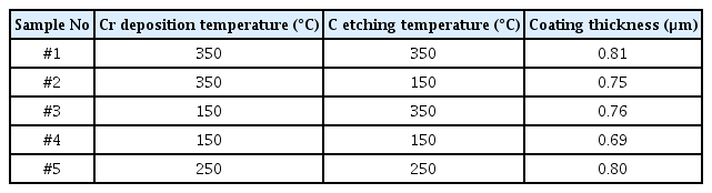
Coating thickness at different combinations of Cr deposition and subsequent C etching temperatures
Figure 4 shows the hardness measured using the nanoindentation tester. Slight variations in sample hardness (1,225–1,576 HV) are observed at different temperature combinations. A significant decrease in hardness was observed at the temperature combination of 150-350 (sample #3); however no specific trends or associations were observed for the Cr deposition and C etching temperatures. The deviation in hardness can be attributed to the substrate material and deposition thickness. The substrate material is a sintered body of fine, ultra-hard WC particles and Co binder; therefore, a deviation in the dispersion state of WC at a micro area is speculated. In addition, the deposition thickness was extremely thin (0.69–0.81 µm).

Hardness variation according to Cr deposition and subsequent C etching temperature combinations
Figure 5 shows a cross-section of the Cr(C) interface layer, obtained using a calotte tester. In all samples, a white Cr layer was observed on the cemented carbide substrate and a C etching layer formed on the top. A black-grey interfacial layer of Cr(C) mixing layer (or reaction layer) from Cr and C formed between these two layers, which can be observed clearly in sample #1 (350-350). At other temperature combinations, the Cr(C) layer is not clearly seen during the calotte test. Although the appearance of the Cr(C) layer is different in all samples, the layer is partially visible in all of them. Therefore, the diffusion reaction of C into the Cr layer is speculated to progress to a certain extent by the C etching process after Cr deposition.

Cross sectional microstructure images, obtained by calotte tester, of the Cr-C interface with various temperature combinations (1,000x)
Figure 6 demonstrates the XRD patterns of the Cr(C) interfaces, produced using different temperature combinations of Cr deposition and C etching on Si wafer. An incident angle of 6° was applied to exclude the effects of matrix noise. No carbide peak was observed in any form, except in the typical crystalline metal Cr at 42°, 43.5° and 51°, regardless of the combination of treatment temperatures. Therefore, the black-gray Cr(C) interface, observed in Fig 5, can be attributed to the penetration and diffusion of a fraction of C into the Cr layer.

X-ray diffraction pattern of the Cr(C) interfaces, Cr deposited and subsequently C etched using various temperature combinations
3.2. Effect of CH4 addition on Cr(C) interface during Cr deposition
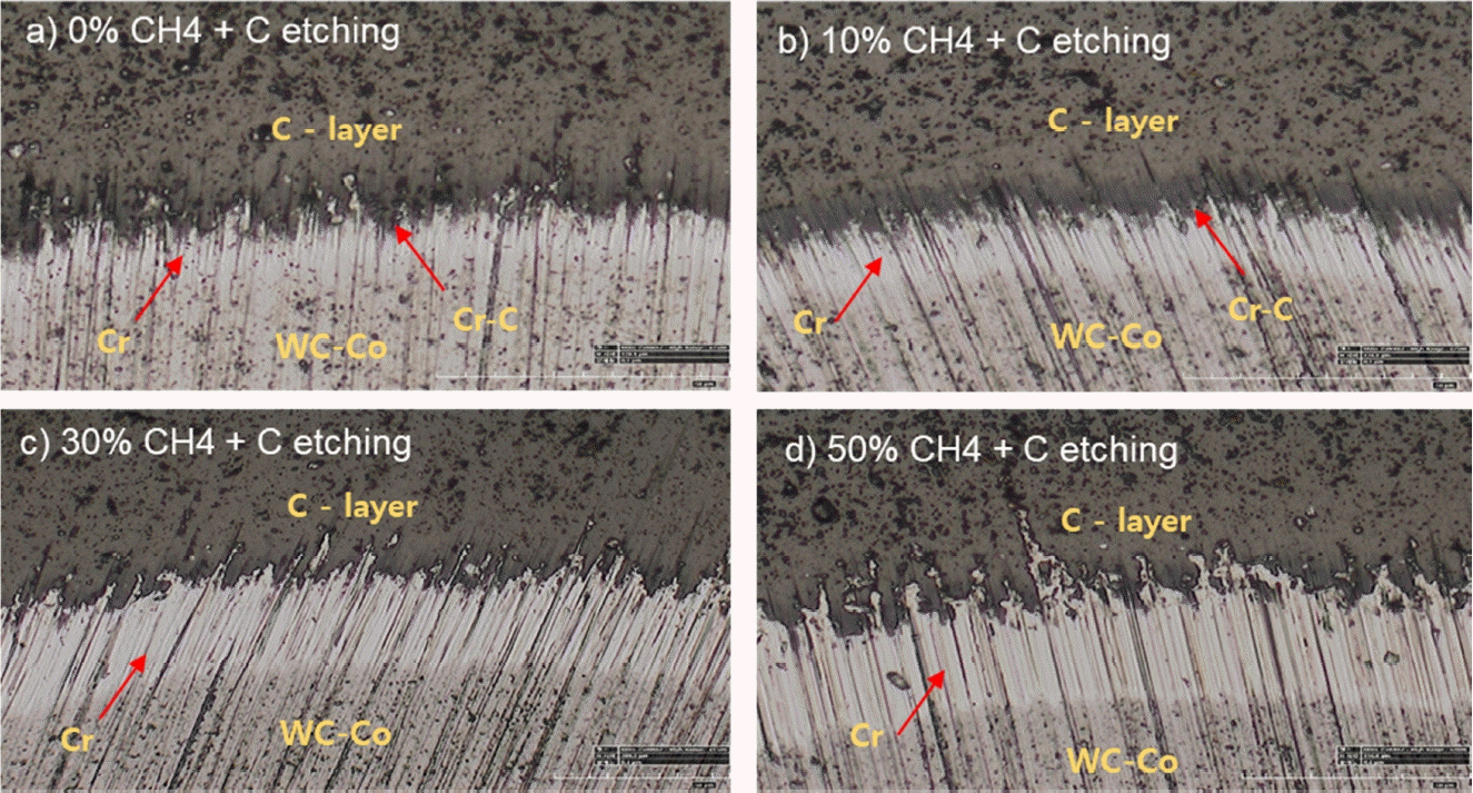
Figure 7 presents cross-sectional photographs obtained using a Calotte tester, to observe the effect of the amount of CH4 input during the Cr deposition process on the Cr(C) interface. No significant difference is observed up to 30% CH4. However, the Cr coating layer interface as indicated by arrow, changes to a slightly dark color at 50% CH4. According to the Cr-C phase diagram (Fig 1a), the liquidus temperature decreases rapidly with increasing C in Cr, which is related to the increase in the solid-solution limit of C in Cr.

Optical micrographs cross-sectional images, obtained by calotte tester, of the Cr(C) interface, Cr deposited with various CH4 contents (1500x)
Figure 8 shows the XRD pattern of the Cr-deposited specimens on Si wafer with different CH4 content. A typical crystalline Cr peak is observed when only Cr was deposited without CH4 input, whereas various Cr carbide peaks, such as Cr7C3 (124, 108, 411) and Cr23C6 , with low intensity are observed at different amounts of CH4 input. Moreover, the peaks with the least intensity are seen when the CH4 input is 50%. The crystalline Cr peak nearly disappears with the addition of CH4, indicating that the matrix cannot be crystallized by CH4 and remains in an amorphous state.
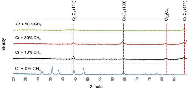
X-ray diffraction patterns of the Cr(C) interface, Cr deposited with various CH4 contents.
Although CH4 input slightly promoted Cr carbide precipitation, this did not affect the crystallization of the matrix, thereby allowing it to remain amorphous.
3.3. Effect of subsequent C etching on the Cr(C) interface, Cr deposited with various contents of CH4
The experimental data, discussed in previous sections, confirmed that a certain amount of C could be added into the Cr interface layer by introducing CH4 during Cr deposition. However, this artificial addition has helped with some Cr carbide precipitation in the Cr deposition layer, but on the other hand, there is even the possibility of keeping the Cr(C) interface in a fragile amorphous state, so the focus is naturally on how to improve it.
Figure 9 shows the XRD patterns of Si wafer specimens, which were C-etched after the Cr deposition process in the presence of CH4. Comparing this with Fig 8 (before C etching), we can see that the intensity of the peak corresponding to Cr7C3 carbide increases slightly. The highest intensity Cr7C3 peak is observed when the CH4 input is 10%, indicating that the subsequent C etching process with high energy facilitates the supersaturated C in the Cr(C) interface, which participates in the Cr7C3 carbide precipitation. In other words, the subsequent C etching process imparts a tempering effect. Furthermore, this suggests the possibility of an additional tempering effect in the thick TAC film deposition process, which is conducted for a long duration as another process, subsequent to the C etching process.
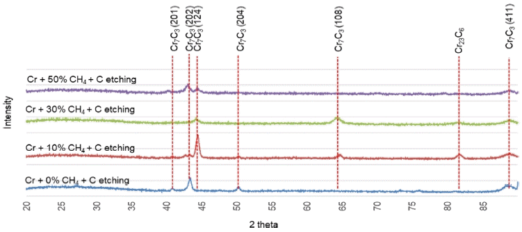
X-ray diffraction patterns of the Cr(C) interfaces, Cr deposited with various CH4 contents and subsequently C etched
Figure 10 demonstrates the effect of the subsequent C etching process on the hardness of the Cr(C) interface, developed on Cr-deposited cemented carbide specimens with various CH4 input. The Cr deposition, and subsequent C etching without CH4 input, results in an increase in hardness of approximately 350 HV, while the hardness is decreased approximately 10% by the subsequent C etching when CH4 is introduced. The results agree well with the XRD pattern (Fig 8), where the hardness increases with Cr deposition and C etching without CH4 input. This is attributed to the penetration and diffusion of activated carbon ions into the Cr layer during the subsequent C etching process, which leads to an increase in hardness because of the strengthening of the solid-solution.

Effect of subsequent C etching on the hardness of the Cr(C) interface, Cr deposited with various CH4 contents
In contrast, when CH4 is added during the Cr deposition, the amorphization of the Cr matrix accelerates in proportion to the amount of the CH4 input, and a steep rise is observed. Further, the subsequent C etching process with high energy tempers the Cr matrix. This leads to a simultaneous precipitation of Cr carbide and crystallization of the matrix, thereby lowering the hardness.
Figure 11 shows the cross-sectional photographs obtained by a calotte tester to examine the effect of Cr deposition at different CH4 contents, followed by the C etching process on the Cr(C) interface. The width of the white Cr deposition layer is observed to increase gradually with increasing CH4. This indicates an increase in the amorphization and brittleness of the matrix due to the increased C content in the Cr matrix, thereby increasing damage to the Cr(C) interface during rotating vibration.
Cross-sectional optical micrographs, obtained by calotte tester, to examine the effect of subsequent C etching on the Cr(C) interface, coated with Cr at various amounts of CH4 (1000 x)
Figure 12 depicts the results of EDS analysis of the surface of the Cr(C) interface, to examine the changes in the Cr and C contents before and after C etching. Before C etching, the C content increases in proportion to the increasing CH4 content, whereas the Cr content decreases constantly. However, after C etching, the C content decreases with increasing CH4 content and exhibits a peculiar tendency to increase again at 50% CH4. A similar trend is observed in Cr, which decreases constantly and increases again at 50% CH4.

EDS analysis showing the Cr and C trends before (a) and after (b) C etching of the Cr(C) interface, Cr deposited with various CH4 contents
It is speculated that most of the C is well dissolved in the Cr before C etching; however, during the etching process, the solution of C activated in a high energy state increases, up to approximately 30% CH4 content, due to penetration and diffusion in the Cr. When the CH4 content reaches 50%, the C enters into a supersaturated state and then discharges to the surface. This is consistent with the Cr-C phase diagram shown in Fig 1. This phenomenon can be confirmed with the SEM surface micrographs, shown in Fig 13.

SEM micrographs showing before (a–d) and after (e–h) C etching (C*) of the Cr(C) interface Cr coated with various CH4 contents
When there is no CH4 input during Cr deposition (Fig 13a), Cr particles, as indicated by arrows, are deposited on the coating surface in a stacked form, while the coating surface has a very smooth amorphous appearance in the presence of 10% CH4 (Fig 13b), which is significantly different from that shown in Fig 13a. A few dimples as indicated by arrows are observed to gradually develop on the smooth surface with increasing CH4 content (Fig 13c and 13d). The observations suggest lattice warping, or strain energy induced by excessive solution of C in the Cr matrix, is transferred to and accumulated in the grain boundary, resulting in the formation of dimples as intergranular protrusions.
However, the amorphous smooth surface and dimples are not observed after subsequent C etching (Fig 13e–13h), likely because the Cr(C) surfaces are covered by a C layer and C droplets during the subsequent C etching process.
Figure 14 illustrates the fractures in the cross-sections of the Cr(C) surfaces structures. A general cleavage fracture surface of the ultra-hard crystalline metal is observed (Fig 14a) when CH4 is not added before subsequent C etching. Smooth and brittle fracture surfaces frequently appear in ultra-hard amorphous structures when the amount of CH4 is increased gradually (Fig 14b–14d). In contrast, all of the samples after C etching exhibited similar compromised fracture shapes of cleavage, and smooth fracture surfaces.

SEM micrographs to show the cross-section before (a–d) and after (e–h) C etching (C*) of the Cr(C) interface Cr coated with various CH4 contents
This suggests that softening of the matrix occurred with the tempering effect due to the kinetic energy, accelerated with high energy by 900V, during the subsequent C etching process [13]. The results indicate that the subsequent C etching process, and the addition of CH4 during Cr deposition, significantly affect the structure and physical properties of the Cr(C) interface layer. Therefore, identifying the correlation between this phenomena and the adhesion of the Cr(C) interface is crucial.
Figure 15 demonstrates the adhesion force, which was measured before and after C etching on the Cr(C) interfacial layers deposited with various amounts of CH4 during the Cr coating, using a scratch tester. A maximum load of 50 N was set for all to avoid breaking the stylus during the test. Consequently, it was found that all of the samples with only a Cr(C) layer before C etching exceeded 50 N, regardless of the amount of CH4 during the Cr deposition process. In contrast, all samples exhibited adhesion in the range of 29–35 N after C etching. Nevertheless, the Cr(C) layer, which is the lower layer, maintained the same shape as before the C etching inside the track. This is in good agreement with the SEM cross-sectional analysis (Fig 14), suggesting the two-layer structure of the C etched layer and Cr(C) interfacial layer located immediately beneath the C etched layer.

Optical micrographs of the scratch tracks before (a–d) and after (e–h) C etching of the Cr(C) interface Cr coated with various CH4 contents.
Furthermore, the scratch test confirmed that even if the weak upper layer, i.e., the C etching layer, is damaged under a relatively low load, the lower Cr(C) layer maintains good adhesion. Fig 16 schematically shows the results of adhesion measured between the Cr(C) layer (lower layer) and the C-etch layer (upper layer), as confirmed through the scratch test. In the 29–35 N load range, the damaged C etching layers are partially removed by sputtering during ta-C thick film coating, which is another subsequent process; however, most of them are absorbed and contribute to the layer formation [5,14].

Scratch test results of Cr(C) lower layer before (a) Cr deposition with various CH4 contents; and the C etching layer as the upper layer after (b) Cr deposition, eventually the former of exceeding 50 N and the latter of 25~35 N range respectively.
3.4. Effect of CH4 introduced during Cr deposition on the adhesion of thick TAC film
Figure 17 provides an EDS profile of the fracture surface of the test piece, deposited with Cr at various CH4 content, followed by C etching and thick ta-C coating to investigate the distribution of C and Cr across the interface Cr(C) with 0.4 µm thickness.

EDS profile showing the distribution of C and Cr across the interface, Cr deposited with various CH4 contents, subsequently C etched and thick TAC coated.
A homogeneous distribution of Cr is observed with a nearly constant EDS intensity across the Cr(C) interface and TAC layer, regardless of the CH4 input. In contrast, a sharp increase in C content is observed from the cemented carbide substrate to the TAC layer through the Cr(C) interface. The C content increases in proportion to the increase in CH4 input. Thus, C, introduced in the form of CH4 during Cr deposition continues to diffuse toward the TAC deposition film during the subsequent C etching and TAC deposition processes. Consequently, the precipitation reaction of Cr carbides in the TAC deposition film is speculated to be more active. Furthermore, the C diffuses into the Cr interface layer during the C etching process, even without CH4 input during Cr deposition; however, the extent is insignificant compared to that with the CH4 input during Cr deposition.
Figure 18 shows the calotte cross-sections (Fig 18a–18d) and the optical images of the Rockwell indentations (Fig 18e–18h) of carbide specimens, prepared in advance, to observe the effect of Cr deposition with CH4 on the adhesion of the TAC thick film. Considering the hardness level and coating thickness of the ta-C coating layer, measuring the adhesion using a scratch tester was not possible; therefore, the Rockwell indentation method was adopted with a load of 150 kg.

Optical images of the coating thickness and adhesion force of TAC layer according to CH4 contents during Cr deposition. Thickness was measured by calotte tester (upper) and adhesion by Rockwell indentation (lower).
Most of the measured coating thicknesses were observed to be within the range 5.27–5.42 µm. Furthermore, the coating adhesion showed HF1 grade, regardless of the type, and as a result it was not possible to distinguish between superior and inferior. The Rockwell indentation method did not create sufficient shear stress to separate the TAC thick film from the cemented carbide substrate; therefore, a new method was designed.
Figure 19 shows the evaluation results following the use of a sand blasting device, which was designed to measure adhesion better than the Rockwell indentation method. The analysis was performed with a projection pressure of 3 bar, projection time of 120 s, and projection distance of 10 mm using white alumina with a particle size of 110 μm as the projection media.

Optical images showing adhesion after sand blasting of the thick TAC multi-layers deposited with various CH4 contents during the Cr deposition process. Consequently, the peel-off rates were a) 91%, b) 4%, c) 0.01%, d) 0.4%, respectively, as determined by image analysis.
Superior and inferior adhesion could be clearly distinguished based on the amount of CH4 input during Cr deposition. Samples with CH4 content exhibited better adhesion than those without CH4 content. Samples obtained with 30% CH4 during Cr deposition show the most remarkable results, in good agreement with the previous test results, such as the highest hardness value at 30% CH4, the highest solid solution of C in Cr (EDS analysis), and the maximum precipitation of Cr carbides, particularly Cr7C3.
Briefly, the Cr matrix showed a tendency to be vulnerable to amorphization at the time of Cr deposition due to the addition of CH4 ; however, the amorphous matrix was affected by the tempering effect during the subsequent C etching process with strong energy, followed by the relatively long duration TAC deposition process. The crystallization and the precipitation reaction of the Cr carbide and the stabilization of the interface progressed because of the reduction in internal stress, and consequently, the adhesion of the interface increased significantly.
Figure 20 shows the SEM microstructure of the cross-sectional fracture of the multi-layered thick ta-C coating with 30% CH4 input during Cr deposition. Fig 20a illustrates a multilayer thick TAC film, while Fig 20b is an enlargement of the dotted circle in Fig 20a, where the Cr(C)-C interface can be clearly distinguished. The total thickness of the TAC multilayer is 5.3 μm and the thickness of the double interfacial layer is 0.4 μm.

SEM cross-sectional micrographs of thick TAC multi-layer deposited with 30% CH4 during Cr deposition, a) thick TAC multilayer (5.3μm coating thickness, 51.6 GPa hardness by nanoindentation), b) magnified microstructure in the dotted circle of a).
The TAC multilayer has two colors; the two hardness layers were alternately laminated by varying the bias voltage during coating, to lower the internal compressive stress.
Figure 21 shows the results of Raman analysis, performed three times for the TAC thick film of the multilayer structure deposited with 30% CH4 during Cr coating. The two peaks with full-wide-half-maximum widths are at approximately 1350 cm-1 (I(D) peak) and 1580 cm-1 (I(G) peak), which overlap each other. Their relative ratio, I(D)/I(G) value, is calculated to be in the range 0.64–0.72, which represents a typical ultra-hard TAC coating layer structure [15–17].

Raman analysis of thick TAC multi-layer coated with 30% CH4 during Cr deposition.
4. CONCLUSIONS
CH4 was introduced during the Cr deposition process to observe the interfacial behavior with the cemented carbide substrate, and to improve the adhesion of the thick TAC film. The following conclusions were obtained:
Hardness measurements and XRD analyses were performed on the samples, prepared using various combinations of Cr deposition temperature and C etching temperature in the range 150–350 °C, to observe the Cr-C interface reaction. No specific trend was observed except for local deviations, which was attributed to the use of WC dispersed material as a substrate, and the extremely thin 0.69–0.81 µm coating.
The artificial addition of CH4 during the Cr deposition process, to promote the reaction of Cr and C at the Cr-C interface, resulted in the precipitation of CrxCy-based carbides, including the Cr7C3 phase. An increase in hardness was observed with increasing CH4 content; however, the hardness decreased slightly when the CH4 input reached 30%.
In the C etching and TAC process, performed after Cr deposition with various CH4 contents, precipitation of the Cr7C3 phase and crystallization of the matrix were promoted by the tempering effect of the Cr(C)-C interface, and a remarkable improvement in adhesion was observed, particularly when the CH4 content reached 30%.
Acknowledgements
This work was supported by “Human Resources Program in Energy Technology” of the Korea Institute of Energy Technology Evaluation and Planning (KETEP), granted financial resource from the Ministry of Trade, Industry & Energy, Republic of Korea. (No. 20214000000200) and the National Research Foundation of Korea (NRF) grant funded by the Korea government (MSIT) (No. NRF2021R1A5A8033165).
Notes
The authors declare no conflict of interest.