


1. INTRODUCTION
Thermoelectric materials directly convert waste heat into electricity via the Seebeck effect [1-3]. The performance of thermoelectric materials is evaluated by thermoelectric figure of merit, zT = σS2T/κtot; here σ, S, T, and κtot denote the electrical conductivity, Seebeck coefficient, absolute temperature, and total thermal conductivity, respectively [4,5]. The κtot is the sum of electronic thermal conductivity κelec and lattice thermal conductivity, κlatt. To achieve a high zT, a high value of σS2 (power factor) and a low κtot are required. However, the complex trade-off relation among σ, S, and κelec hinders enhancing zT of thermoelectric materials. Despite these obstacles, strategies to enhance zT by improving σS2 via carrier concentration optimization or by reducing κlatt via phonon scattering caused by additional point defects have been attempted for conventional thermoelectric materials, such as Bi2Te3- and PbTe-based alloys [6-9].
Recently, metal dichalcogenides have been studied extensively owing to their unique electronic and optical properties [10-12]. Among those, post-transition metal chalcogenides, such as InSe [13], SnSe [14], and SnSe2 [15-17] have been investigated as promising thermoelectric materials. SnSe2 has a CdI2-type layered structure and has attracted considerable attention as a promising n-type thermoelectric material [18,19]. However, it has a low carrier concentration, resulting in low values of σS2 and zT. Thus, the effect of increasing the carrier concentration on zT has been subsequently studied. Ding et al. predicted that a maximum zT of 2.95 at 800 K can be obtained in the a-axis direction with a carrier concentration of 1 × 1020 cm–3 [20]. Kim et al. reported that substitutional doping of Br at the Se site in SnSe2 resulted in a high zT of 0.62 at 750 K, along with an increase in the carrier concentration to approximately 1019cm–3 [17].
In this study, we employed Sb as a dopant for Se site in SnSe2 to increase its carrier (electron) concentration. Choe et al. reported that Sb doping of the Se site of SnSe2 increased the electron concentration from 7.40 × 10¹⁷ to 1.50 × 1019 cm–3 significantly; this was facilitated by the donor-like behavior of Sb at the Se site [21]. They found that Sb doping in the Se site provides electrons as Sb doped as metal with the oxidation number almost ~0 based on the Bader net charge distribution analysis [21]. (Note that either Sb3+ doping in Sn site of SnSe2 or Sb3-doping in Se site of SnSe2 cannot generate electrons.) Thus, herein, we prepared a series of Sn(Se1–xSbx)2 to systematically investigate the influence of Sb doping on the thermoelectric transport properties of SnSe2 to further understand the Sb doping in Se site in SnSe2. It was observed that the electron concentration increased significantly with Sb doping. In addition, the thermoelectric transport properties of the Sb-doped SnSe2 samples were analyzed using density-of-state effective mass, md*, weighted mobility, μw, and thermoelectric quality factor, B.
2. EXPERIMENTAL PROCEDURES
Polycrystalline Sn(Se1–xSbx)2 samples (x = 0, 0.015, 0.03, 0.045, and 0.06) were synthesized using a solid-state reaction method. Stoichiometric amounts of Sn, Se, and Sb were weighed and vacuum-sealed in a quartz tube. The vacuumsealed quartz tubes were heat-treated at 1073 K for 8 h, then quenched with cold water, and annealed at 850 K for 72 h. The obtained ingots were pulverized for 5 min by high energy ball milling in an Ar atmosphere. The crystal structures of the powders were characterized by X-Ray diffraction using CuKα1 radiation (XRD, D8 Discover, Bruker). XPS analysis were carried out with X-ray spectrometer (Nexsa G2 XPS, Thermo Scientific) using a focused monochromatized Al Kα radiation. The powders were densified via spark plasma sintering at 10–6 Torr and 707 K for 10 min. The σ and S values were measured by a thermoelectric evaluation system (ZEM-3M8, Advance Riko, Japan) in the temperature range of 300–790 K. Measuring direction was along the perpendicular direction of SPS pressing direction. The Hall measurement of each sample was performed using a Hall measurement system under a magnetic field of 0.553 T (HMS5300, Ecopia). Thermal diffusivity, α, required to obtain κtot (κtot = α × ρs × Cp, where ρs and Cp are the sample density and heat capacity, respectively) was measured by the laser flash method (LFA457, Netzsch) in the temperature range of 300–790 K. Measuring direction was along the perpendicular direction of SPS pressing direction. ρs of the samples was calculated by Archimedes` method.
Table 1 shows relative density of sintered samples. Relative density of samples was calculated via dividing ρs by theoretical density of hexagonal SnSe2, i.e., 5.950 g/cm3 [22]. Cp was calculated based on the following empirical relationship [23]: Cp = 73.39 + 1.15 × 10⁻² T – 1.92 × 10⁵ T-2 J/mol·K. As the doping concentrations of the samples were significantly low, the changes in Cp from the Sb doping were considered negligible. Following the data measurements, zT values were calculated.
3. RESULTS AND DISCUSSION
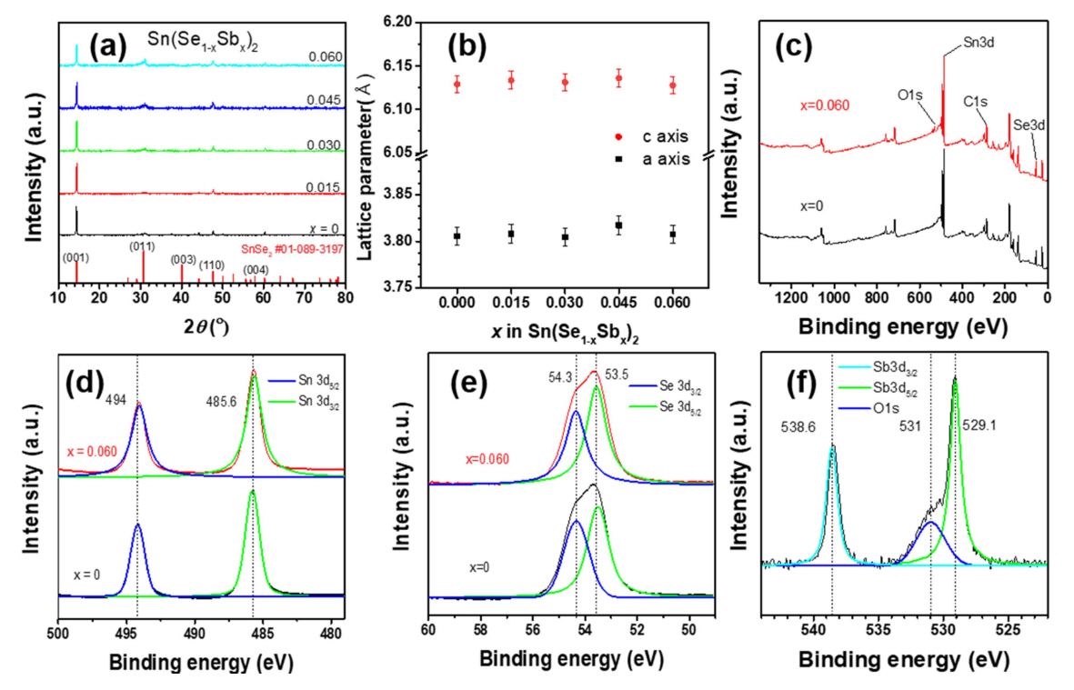
Fig 1(a) presents XRD peaks of the pulverized Sn(Se1–xSbx)2 samples. The XRD patterns show that the hexagonal SnSe2 samples were synthesized without any additional phases. The lattice parameters were calculated using the (001) and (110) diffraction peaks (Fig 1(b)); it was observed that there was no significant change in the lattice parameters. Fig 1(c) shows the XPS spectra of the Sn(Se1-xSbx)2 (x = 0 and 0.06) samples, which shows presence of Sn 3d, Se 3d peaks. Fig 1(d) and Fig 1(e) show high resolution XPS peaks of Sn 3d and Se 3d respectively. The XPS peaks of Sn 3d3/2, Sn 3d5/2, Se 3d3/2 and Se 3d5/2 are located at 494.0, 485.6, 54.3 and 53.5eV, respectively, which is in good agreement with prior study of polycrystalline SnSe2 [24]. Fig 1(f) shows high resolution Sb 3d XPS spectra of Sn(Se1-xSbx)2 (x = 0.06), which shows presence of Sb peaks. Overlap of the O 1s peak and Sb 3d5/2 peak indicates physiosorbed oxygens at the surface. The Sb 3d5/2 peak of the Sb-doped SnSe2 sample appears at binding energy of 529.1 eV, which is close to the binding energy of 528.3 eV of metallic antimony (Sb0) [25].
Fig 2(a) and 2(b) show σ and S as functions of temperature. The σ values of the Sb-doped samples increased with increasing Sb content, except for x = 0.015. As shown in Fig 2(a), the σ values at 300 K for x = 0, 0.015, 0.03, 0.045, and 0.06 were 6.35, 3.60, 13.2, 29.5, and 81.4 S/cm, respectively. The values of S of all the samples were negative over whole temperature range, thus establishing the n-type conduction behavior of the samples. The absolute S of the undoped sample (x = 0) generally decreased with temperature. In contrast, the absolute S of all the doped samples increased with temperature. At 300 K, the magnitude of S for x = 0.015 decreased significantly to –130 μV/K compared with –438 μV/K of the pristine sample. Moreover, the magnitude of S gradually decreased to –127, – 103, and –103 μV/K for x = 0.03, 0.045, and 0.06, respectively. At 750 K, the S values changed rather gradually to –377, –285, –217, –189, and –150 μV/K for x = 0, 0.015, 0.03, 0.045 and 0.06, respectively. Fig 2(c) shows the calculated power factor σS2 as a function of temperature for the Sn(Se1–xSbx)2 samples. The power factor values of Sbdoped samples decreased compared to that of the pristine sample at all temperatures. Moreover, σS2 decreased significantly at the low doping level of x = 0.015 and generally increased x > 0.015. The significant decrease in σS2 for x = 0.015 could be attributed to the large reduction in the magnitude of S (Fig 2(b)).
Next, μw was calculated and displayed in Fig 2(d) as a function of temperature. μw refers to theoretical maximum power factor that can be obtained by optimizing carrier concentration [26] and can be analytically calculated from the Drude–Sommerfeld free-electron model for |S| > 20 μV/K [25]:
where h and me denote Planck’s constant and electron mass, respectively. As shown in Fig 2(d), μw was reduced significantly for the doped samples. For instance, at 300 K μw values were 44, 0.69, 2.4, 4.0, and 11 cm2/V∙s for x = 0, 0.015, 0.03, 0.045, and 0.06, respectively. At 750K, the corresponding values were 23, 8.0, 7.6, 6.8, and 7.9, respectively. The undoped sample had the highest μw among all the samples over the entire temperature range, and it increased with increasing Sb doping, following the same trend as σS2 (Fig 2(c)).
Fig 3(a) and 3(b) present Hall carrier concentration, nH and Hall carrier mobility, μH at 300 K for Sn(Se1–xSbx)2 as functions of x. The values of nH were 2.17 × 10¹⁸, 4.17 × 10¹⁹, 6.91 × 10¹⁹, 7.14 × 10¹⁹, and 8.44 × 1019 cm–3 for x = 0, 0.015, 0.03, 0.045, and 0.06, respectively. Furthermore, nH increased significantly at the low doping level of x = 0.015 and gradually increased for x beyond 0.015. This result indicates that the Sb metal with the oxidation number ~0 doped into the anion site of SnSe2 so Sb0 in Se2-site acts as an electron donor, which is reported in ref. [21] based on the Bader net charge calculations. The small difference of electronegativity and long bond length between Sn and Sb hindered the effective charge transfer of the Sn–Sb bond, which could validate the oxidation number of the Sb atoms to become approximately 0, which is known from Bader net charge calculation [21]. Thus, the Sb in Se sites in our samples of Sn(Se1–xSbx)2 behaves as electron donors.
As shown in Fig 3(b), μH was significantly reduced for the doped samples (0.36, 0.86, 2.6, and 5.5 cm2/Vs for x = 0.015, 0.03, 0.045, and 0.06, respectively), as compared with 17 cm2/Vs for the undoped sample. The large reduction of μH is also seen for Sn(Se0.96Sb0.04)2 composition. in ref [21].
Fig 3(c) shows the calculated md* of Sn(Se1–xSbx)2 samples based on a single parabolic band model under the acoustic phonon scattering mechanism [27]:
where md* and n denote the effective density-of-state mass and carrier concentration, respectively. The inset graph of Fig 3(c) shows logarithmic nH as a function of |S|. The md* values of the doped samples were 0.94, 1.28, 1.05, and 1.17 m0 for x = 0.015, 0.03,0.045, and 0.06, respectively; these were lower than 1.48 m0 for x = 0. Both md* and μw (Fig 2(d)) decreased with Sb doping, suggesting that the electrical transport properties were degraded by Sb doping in SnSe2.
Fig 4(a), 4(b), and 4(c) present κtot, κelec, and κlatt, respectively. κelec of the samples was calculated using the Wiedemann–Franz law [28] as follows: κelec = LσT, where L denotes the Lorenz number and is calculated using the following equation [29]:
κlatt is obtained by subtracting κelec from κtot. As the measured κelec of the samples was extremely small owing to low σ values, κlatt was nearly equal to κtot. The values of κlatt of the doped samples were 2.64, 2.21, 1.94, 1.81, and 1.13 W/mK at 300 K and 0.91, 0.82, 0.76, 0.86, and 0.54 W/mK at 750 K for x = 0, 0.015, 0.03, 0.045, 0.06, respectively. Moreover, κlatt noticeably decreased with doping, indicating that Sb doping increased point defect scattering.
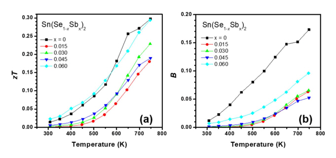
Fig 5(a) shows the calculated zT values as functions of temperature. In general, no noticeable zT enhancement was observed upon doping. zT was decreased significantly by low-level doping of Sb (x = 0.015); then, for x = 0.06. zT gradually recovered to the value of the undoped sample. The large reduction in zT could be attributed to the large reduction in σS2; moreover, the gradual increase in zT beyond x = 0.15 was owing to the modest recovery of σS2 (Fig 2(c)) and the reduction in the thermal conductivities (Fig 4(a) and 4(c)). No enhancement of zT could be achieved in the Sb-doped Sn(Se1–xSbx)2 samples in the x range of 0.015–0.06. Fig 5(b) shows B of each sample, which was calculated using the following equation [30]:
B is proportional to maximum zT when nH is optimized. The values of B for x = 0, 0.015, 0.03, 0.045, and 0.06 were 0.0120, 0.0002, 0.0009, 0.0016, and 0.0070, respectively at 300 K and 0.170, 0.060, 0.066, 0.052, and 0.096, respectively at 750 K. Generally, B of Sb-doped sample was lower than that of pristine SnSe2. Sb doping in SnSe2 successfully and significantly increased the electron concentration, and reduced the thermal conductivities; however, the overall thermoelectric transport properties were not enhanced owing to reduction of md* and μw.
4. CONCLUSIONS
In this study, a series of Sn(Se1–xSbx)2 (x = 0, 0.015, 0.03, 0.045, and 0.06) polycrystalline samples was synthesized and their thermoelectric transport properties were investigated. Electrical conductivity was generally enhanced by Sb doping owing to a large increase in the electron concentration; in contrast, the Seebeck coefficient was largely decreased by doping. Consequently, the power factor for the lowest doping (x = 0.015) was significantly decreased from 0.37 mW/mK2 of the pristine samples at 600 K to 0.21 mW/mK2. The power factor generally increased as the Sb doping increased from x = 0.015. The density-of-state effective mass and weighted mobility decreased with Sb doping, suggesting that the electrical transport properties were consequently degraded by Sb doping in SnSe2. The total and lattice thermal conductivities gradually decreased owing to additional point defect scattering. Thus, thermoelectric figure of merit at the lowest Sb doping (x = 0.015) decreased significantly from 0.30 of the pristine sample at 750 K to 0.18; subsequently, the thermoelectric figure of merit gradually recovered to the value of the undoped sample at x = 0.06. The thermoelectric quality factor decreased as the Sb doping increased. Sb doping in SnSe2 significantly enhanced the electron concentration and reduced the thermal conductivities; however, the overall thermoelectric transport properties were not enhanced owing to a reduction in the density-of-state effective mass and weighted mobility.