


1. INTRODUCTION
Many important material properties in ferroelectric ceramics, such as hysteresis curves and piezoelectric coefficients, are dependent on ferroelectric domain structures and domain wall motions [1,2]. Understanding of such ferroelectric domain structures at a microscopic scale has been significantly improved due to the development of characterization techniques [3]. Atomic force microscopy (AFM) and electron microscopy are central to the microscopic techniques employed for ferroelectric domains.
Piezoresponse force microscopy (PFM) is one of the most used microscopic techniques to study ferroelectric domain structures [3-5]. PFM works by exciting a local converse piezoelectric effect on the surface of ferroelectric materials using the scanning probe. PFM is a powerful tool for visualizing ferroelectric domains because the PFM signal is generated based on distinct polarization directions. This enables the observation of both 180┬░ and non-180┬░ domain walls. The ability to resolve domain patterns can be further enhanced by taking advantage of three-dimensional PFM (vertical PFM and two orthogonal lateral PFMs) [5] or angleresolved PFM based on lateral signals [6]. In addition, the resolution of PFM can be enhanced by modulating a driving frequency near the contact resonance frequency [7].
PFM has been used to observe the ferroelectric domain wall motions induced by an external electric field using the AFM tip as a movable electrode [8] or scanning on a conductive electrode [9]. However, there has been little PFM study on ferroelectric domain wall motion induced by external mechanical stress. Ferroelectric polarization can be switched by mechanical stress using the AFM tip [10], but this is different from the domain evolution processes generated by external macroscopic mechanical stress. Domain evolution processes in single crystals of BaTiO3 induced by external mechanical stress have been observed using an ex situ PFM technique [11]. Although this work shows polarization switching via domain wall motions, it is not sufficient to understand the evolutionary processes in the complex domain patterns which are formed to minimize the total energy in the microstructure.
In the present study, in situ PFM observation of polycrystalline PZT under compressive stress was conducted to elucidate the domain wall motions of complex domain patterns. Electron backscatter diffraction (EBSD) was used in conjunction with vertical PFM to systematically interpret the domain configurations. Domain evolution processes via two competing sets of lamellations under compressive loading are introduced.
2. EXPERIMENTAL METHOD
Polycrystalline soft PZT near the morphotropic phase boundary (PZT-855, APC international) was cut into 2├Ś4├Ś5 mm3 dimensions, and one of the 4├Ś5 mm2 surfaces was polished for PFM observation. PFM was carried out using a Veeco Dimension 3100 nanoscope. Further details on PFM can be found in the existing literature [6]. The scanning probe, a Bruker SCM-PIC, was used for vertical PFM, and a driving frequency was modulated near the contact resonant frequency (180 ŌĆō 200 kHz). Scanning electron microscopy (Evo LS 15 Environmental Scanning Electron Microscope) with EBSD was used to identify the crystallographic planes of the non-180┬░ domain wall observed in the PFM images. Using three Euler angles obtained from the EBSD measurements, all of the orientations that can be created by the {100} and {110} crystallographic planes intersecting the viewing plane were calculated. Then, these orientations were compared with the non-180┬░ domain wall orientations observed in the PFM images to identify their crystallographic planes.
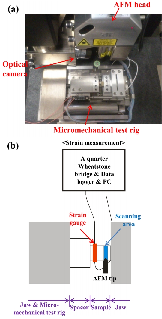
A micromechanical test rig (Deben Ltd.) was fixed to the AFM sample stage controller to precisely control the sample position under the AFM scanning probe. To monitor the realtime strain value under compression, a strain gauge was placed on the same surface where the PFM scan was conducted (Fig 1(a)). The applied stress and measured strain as a function of time are shown in Fig 2. PFM scans were performed four times: before the compression, at 60 MPa, at 70 MPa, and after completely unloading the compressive stress.
At first, the PFM scan and incremental compression were conducted simultaneously. However, the data acquisition through the PFM scan was significantly disturbed by the mechanical noise generated by the motor in the micromechanical test rig. In addition, the scanning region on the sample surface was shifted by the strain generated by the compressive loading. Thus, the PFM scans were performed under a constant stress level. Further details on the experimental method can be found in the existing literature [12].
3. RESULTS AND DISCUSSION
Prior to discussing the results, it is worth introducing the differences between 180┬░ and non-180┬░ domain walls, and domain wall orientations in this PZT sample. Non-180┬░ domain walls are formed due to local residual strain in the crystallites while 180┬░ domain walls are generated by depolarization field [13]. Typical domain walls in ferroelectric materials are electrically and mechanically compatible, so non-180┬░ domain walls tend to form at certain crystallographic planes to satisfy the compatibility conditions [14]. In contrast, there is no habit plane for the 180┬░ domain walls since the spontaneous strain states across a domain wall are identical. As a result, non-180┬░ domain walls are observed as straight lines and 180┬░ domain walls appear as curvy lines on the material surfaces [15,16]. Meanwhile, in a near-morphotropic PZT, both tetragonal and rhombohedral phases can coexist, giving further complexity in this material. In tetragonal and rhombohedral phases, the spontaneous polarization directions are <100> and <111>, respectively. Accordingly, compatible non-180┬░ domain walls are generated at {110} in the tetragonal, and {110} and {100} in the rhombohedral phase.
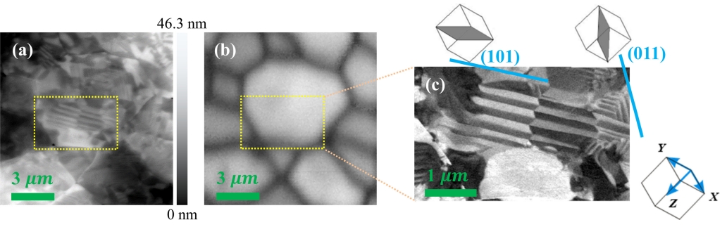
Figures 3(a) ŌĆō (b) show an identical area in an AFM topography image, and image quality map from EBSD, respectively. The root-mean-square roughness (Sq) of the topography image in Fig 3(a) is 7.761 nm. To image the identical grain through AFM and EBSD instruments, the sample surface was systematically traced. First of all, the instrument coordinates in both AFM and SEM were used, and the precision was further enhanced by observing holes and triple junctions on the sample surface through SEM and an optical microscope in AFM. The identical grain was identified using AFM topography image and EBSD image quality map by comparing the shapes and sizes of grain boundaries. It can be clearly confirmed that this is the same region on the PZT sample surface by matching the configuration of grain boundaries in these two images.
PFM scans were carried out during a compressive loading process in the region marked by the rectangle, and the PFM image before compressive loading is shown in Fig 3(c). Using the EBSD data, the crystallographic planes (101) and (011) were distinctively identified for the two sets of differently oriented lamellations. It should be noted that the orientations of the blue lines were computed by intersecting the three-dimensional (101) and (011) crystallographic planes on the viewing plane.
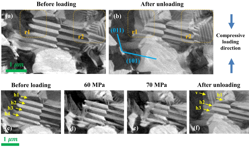
To observe the evolution processes of the domain pattern in Fig 3(c), the PFM scan was conducted while compressing the sample at the stress levels listed in Fig 2. First of all, Figs 4(a) and (b) show the domain structures before compressive loading and after completely unloading. Non-180┬░ domain walls oriented in the (011) and (101) directions can be observed from the PFM images after unloading (Fig 4(b)) as well as before loading (Fig 4(a)). In particular, in the regions marked ŌĆśr1ŌĆÖ and ŌĆśr2ŌĆÖ it can be clearly observed that the domain patterns in the (101) direction were overwritten by the domain patterns in the (011) direction. Figures 4(c)ŌĆō(f) show domain evolution processes, highlighting the large needle-like domain patterns marked by ŌĆśh1ŌĆÖ ŌĆō ŌĆśh4ŌĆÖ. From these four PFM images, it can be noticed that the domain patterns ŌĆśh1ŌĆÖŌĆōŌĆśh4ŌĆÖ were shortened by the growing vertical domain pattern ŌĆśvŌĆÖ in Fig 4(f). In addition, the needle-like domain ŌĆśh4ŌĆÖ vanished from the PFM image after unloading compressive stress.
Based on these observed domain evolution processes, several points can be discussed. First of all, the horizontal needle-like domain pattern in the (101) direction (ŌĆśh1ŌĆÖŌĆōŌĆśh4) was overwritten by the vertical domain pattern in the (011) direction (ŌĆśvŌĆÖ) following external compressive stress. This indicates that polarization switching by external mechanical stress took place following the evolution of pre-existing patterns of domains [12]. Therefore, polarization switching by external mechanical stress occurs not just to lower the energy state of the individual domain, but to lower the total energy of two neighbouring domains across non-180┬░ domain walls.
Secondly, the vertical domain pattern marked by ŌĆśvŌĆÖ suddenly grew in Fig 4(f) after completely unloading external compressive stress. However, it is unlikely that these domain patterns grew due to the removal of mechanical stress. In the experiment, it took several minutes to completely unload the external compressive stress after imaging Fig 4(e), and hence it is speculated that the domain pattern ŌĆśvŌĆÖ grew due to the compressive stress during this unloading process. In addition, using EBSD data in conjunction with PFM enabled the identification of the crystallographic planes for the non-180┬░ domain walls. However, the coexistence of tetragonal and rhombohedral phases in this PZT sample did not allow further analysis for the relationship between polarization directions and the applied compressive loading direction.
Finally, although domain evolution processes for each stress and strain level were observed using PFM, this does not necessarily indicate that the macroscopic stress and strain correspon d to the microscopic stress and strain exerted on the grain shown in Figs 3 and 4. When a compressive stress is applied to polycrystalline PZT, it is speculated that the effective stress exerted on each grain are different from one another, depending on the configuration of the grains. Therefore, in this work the measured stress and strain were used to roughly estimate the effective stress and strain values of the grain that was being observed.
4. CONCLUSION
In this work, domain evolution processes of a near-morphotropic PZT underexternal compressive stress were studied using in situ PFM observation and EBSD. The crystallographic planes of a non-180┬░ domain wall were identified by EBSD, but the polarization axes of the observed domains could not be clarified due to the coexistence of tetragonal and rhombohedral phases in this material. In the PFM images, one set of lamellation was overwritten by another set of differently oriented lamellation by external compressive stress. In conclusion, polarization switching by external compressive stress was producedby pattern evolutions based on pre-existing domain patterns.